

5 Enabling Materials By Dimensionality: From 0D to 3D Carbon-Based. . .
173
In principle, scanning tunneling spectroscopy (STS) could give a direct measure of
electronic band gaps. However, in such a case screening effects arising from the
metal substrate on which the CNT is dispersed become important. A model of these
screening effects was tried, but the final error bars are quite large [91]. Therefore,
accessing to electronic band gaps usually relies both on optical measurement and
theoretical modelling.
The edges for fluorescence emission have been measured for several CNTs, and
the dependence on the tube diameter has been fitted with model functions [92, 93].
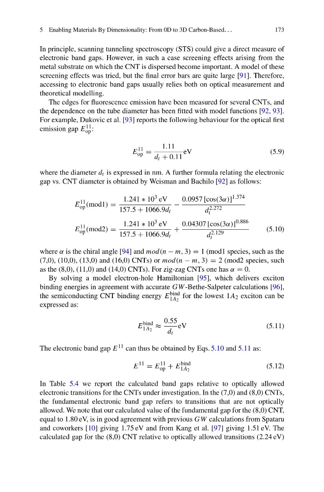
For example, Dukovic et al. [93] reports the following behaviour for the optical first
emission gap E 11
op :
E
11
op =
1.11
d t + 0.11
eV
(5.9)
where the diameter d t is expressed in nm. A further formula relating the electronic
gap vs. CNT diameter is obtained by Weisman and Bachilo [92] as follows:
E
11
op (mod1) =
1.241 ∗ 10 3 eV
157.5 + 1066.9d t
−
0.0957 [cos(3α)]
1.374
d 2.272
t
E
11
op (mod2) =
1.241 ∗ 10 3 eV
157.5 + 1066.9d t
+
0.04307 [cos(3α)]
0.886
d
2.129
t
(5.10)
where α is the chiral angle [94] and mod(n − m, 3) = 1 (mod1 species, such as the
(7,0), (10,0), (13,0) and (16,0) CNTs) or mod(n − m, 3) = 2 (mod2 species, such
as the (8,0), (11,0) and (14,0) CNTs). For zig-zag CNTs one has α = 0.
By solving a model electron-hole Hamiltonian [95], which delivers exciton
binding energies in agreement with accurate GW -Bethe-Salpeter calculations [96],
the semiconducting CNT binding energy E bind
1A 2
for the lowest 1A 2 exciton can be
expressed as:
E
bind
1A 2
≈
0.55
d t
eV
(5.11)
The electronic band gap E 11 can thus be obtained by Eqs. 5.10 and 5.11 as:
E
11
= E
11
op + E
bind
1A 2
(5.12)
In Table 5.4 we report the calculated band gaps relative to optically allowed
electronic transitions for the CNTs under investigation. In the (7,0) and (8,0) CNTs,
the fundamental electronic band gap refers to transitions that are not optically
allowed. We note that our calculated value of the fundamental gap for the (8,0) CNT,
equal to 1.80 eV, is in good agreement with previous GW calculations from Spataru
and coworkers [10] giving 1.75 eV and from Kang et al. [97] giving 1.51 eV. The
calculated gap for the (8,0) CNT relative to optically allowed transitions (2.24 eV)
173
In principle, scanning tunneling spectroscopy (STS) could give a direct measure of
electronic band gaps. However, in such a case screening effects arising from the
metal substrate on which the CNT is dispersed become important. A model of these
screening effects was tried, but the final error bars are quite large [91]. Therefore,
accessing to electronic band gaps usually relies both on optical measurement and
theoretical modelling.
The edges for fluorescence emission have been measured for several CNTs, and
the dependence on the tube diameter has been fitted with model functions [92, 93].
For example, Dukovic et al. [93] reports the following behaviour for the optical first
emission gap E 11
op :
E
11
op =
1.11
d t + 0.11
eV
(5.9)
where the diameter d t is expressed in nm. A further formula relating the electronic
gap vs. CNT diameter is obtained by Weisman and Bachilo [92] as follows:
E
11
op (mod1) =
1.241 ∗ 10 3 eV
157.5 + 1066.9d t
−
0.0957 [cos(3α)]
1.374
d 2.272
t
E
11
op (mod2) =
1.241 ∗ 10 3 eV
157.5 + 1066.9d t
+
0.04307 [cos(3α)]
0.886
d
2.129
t
(5.10)
where α is the chiral angle [94] and mod(n − m, 3) = 1 (mod1 species, such as the
(7,0), (10,0), (13,0) and (16,0) CNTs) or mod(n − m, 3) = 2 (mod2 species, such
as the (8,0), (11,0) and (14,0) CNTs). For zig-zag CNTs one has α = 0.
By solving a model electron-hole Hamiltonian [95], which delivers exciton
binding energies in agreement with accurate GW -Bethe-Salpeter calculations [96],
the semiconducting CNT binding energy E bind
1A 2
for the lowest 1A 2 exciton can be
expressed as:
E
bind
1A 2
≈
0.55
d t
eV
(5.11)
The electronic band gap E 11 can thus be obtained by Eqs. 5.10 and 5.11 as:
E
11
= E
11
op + E
bind
1A 2
(5.12)
In Table 5.4 we report the calculated band gaps relative to optically allowed
electronic transitions for the CNTs under investigation. In the (7,0) and (8,0) CNTs,
the fundamental electronic band gap refers to transitions that are not optically
allowed. We note that our calculated value of the fundamental gap for the (8,0) CNT,
equal to 1.80 eV, is in good agreement with previous GW calculations from Spataru
and coworkers [10] giving 1.75 eV and from Kang et al. [97] giving 1.51 eV. The
calculated gap for the (8,0) CNT relative to optically allowed transitions (2.24 eV)