

172
S. Taioli
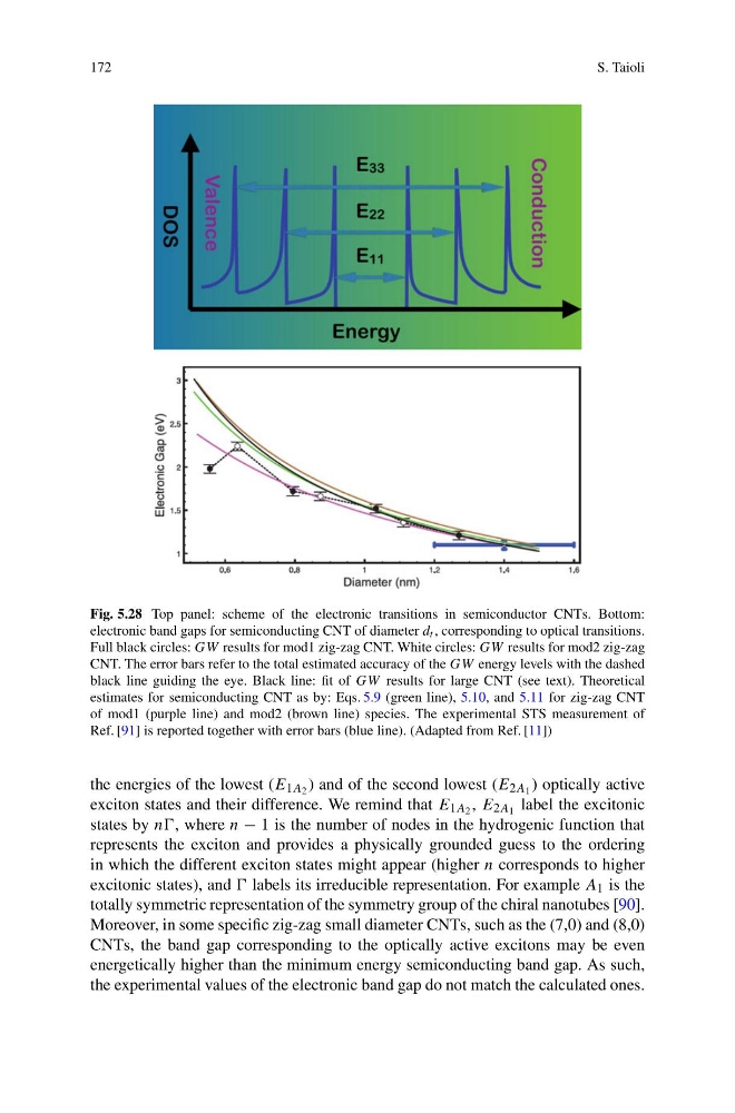
Fig. 5.28 Top panel: scheme of the electronic transitions in semiconductor CNTs. Bottom:
electronic band gaps for semiconducting CNT of diameter d t , corresponding to optical transitions.
Full black circles: GW results for mod1 zig-zag CNT. White circles: GW results for mod2 zig-zag
CNT. The error bars refer to the total estimated accuracy of the GW energy levels with the dashed
black line guiding the eye. Black line: fit of GW results for large CNT (see text). Theoretical
estimates for semiconducting CNT as by: Eqs. 5.9 (green line), 5.10, and 5.11 for zig-zag CNT
of mod1 (purple line) and mod2 (brown line) species. The experimental STS measurement of
Ref. [91] is reported together with error bars (blue line). (Adapted from Ref. [11])
the energies of the lowest (E 1A 2 ) and of the second lowest (E 2A 1 ) optically active
exciton states and their difference. We remind that E 1A 2 , E 2A 1 label the excitonic
states by nn, where n − 1 is the number of nodes in the hydrogenic function that
represents the exciton and provides a physically grounded guess to the ordering
in which the different exciton states might appear (higher n corresponds to higher
excitonic states), and labels its irreducible representation. For example A 1 is the
totally symmetric representation of the symmetry group of the chiral nanotubes [90].
Moreover, in some specific zig-zag small diameter CNTs, such as the (7,0) and (8,0)
CNTs, the band gap corresponding to the optically active excitons may be even
energetically higher than the minimum energy semiconducting band gap. As such,
the experimental values of the electronic band gap do not match the calculated ones.
S. Taioli
Fig. 5.28 Top panel: scheme of the electronic transitions in semiconductor CNTs. Bottom:
electronic band gaps for semiconducting CNT of diameter d t , corresponding to optical transitions.
Full black circles: GW results for mod1 zig-zag CNT. White circles: GW results for mod2 zig-zag
CNT. The error bars refer to the total estimated accuracy of the GW energy levels with the dashed
black line guiding the eye. Black line: fit of GW results for large CNT (see text). Theoretical
estimates for semiconducting CNT as by: Eqs. 5.9 (green line), 5.10, and 5.11 for zig-zag CNT
of mod1 (purple line) and mod2 (brown line) species. The experimental STS measurement of
Ref. [91] is reported together with error bars (blue line). (Adapted from Ref. [11])
the energies of the lowest (E 1A 2 ) and of the second lowest (E 2A 1 ) optically active
exciton states and their difference. We remind that E 1A 2 , E 2A 1 label the excitonic
states by nn, where n − 1 is the number of nodes in the hydrogenic function that
represents the exciton and provides a physically grounded guess to the ordering
in which the different exciton states might appear (higher n corresponds to higher
excitonic states), and labels its irreducible representation. For example A 1 is the
totally symmetric representation of the symmetry group of the chiral nanotubes [90].
Moreover, in some specific zig-zag small diameter CNTs, such as the (7,0) and (8,0)
CNTs, the band gap corresponding to the optically active excitons may be even
energetically higher than the minimum energy semiconducting band gap. As such,
the experimental values of the electronic band gap do not match the calculated ones.