

174
S. Taioli
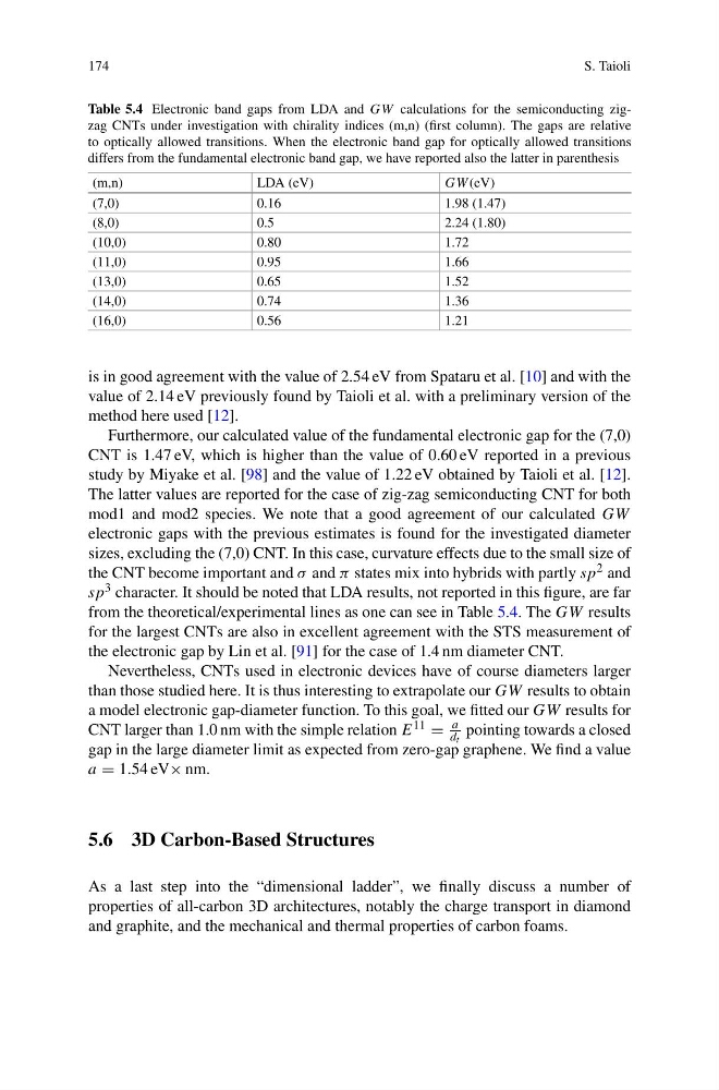
Table 5.4 Electronic band gaps from LDA and GW calculations for the semiconducting zigzag CNTs under investigation with chirality indices (m,n) (first column). The gaps are relative
to optically allowed transitions. When the electronic band gap for optically allowed transitions
differs from the fundamental electronic band gap, we have reported also the latter in parenthesis
(m,n)
LDA (eV)
GW (eV)
(7,0)
0.16
1.98 (1.47)
(8,0)
0.5
2.24 (1.80)
(10,0)
0.80
1.72
(11,0)
0.95
1.66
(13,0)
0.65
1.52
(14,0)
0.74
1.36
(16,0)
0.56
1.21
is in good agreement with the value of 2.54 eV from Spataru et al. [10] and with the
value of 2.14 eV previously found by Taioli et al. with a preliminary version of the
method here used [12].
Furthermore, our calculated value of the fundamental electronic gap for the (7,0)
CNT is 1.47 eV, which is higher than the value of 0.60 eV reported in a previous
study by Miyake et al. [98] and the value of 1.22 eV obtained by Taioli et al. [12].
The latter values are reported for the case of zig-zag semiconducting CNT for both
mod1 and mod2 species. We note that a good agreement of our calculated GW
electronic gaps with the previous estimates is found for the investigated diameter
sizes, excluding the (7,0) CNT. In this case, curvature effects due to the small size of
the CNT become important and σ and π states mix into hybrids with partly sp 2 and
sp 3 character. It should be noted that LDA results, not reported in this figure, are far
from the theoretical/experimental lines as one can see in Table 5.4. The GW results
for the largest CNTs are also in excellent agreement with the STS measurement of
the electronic gap by Lin et al. [91] for the case of 1.4 nm diameter CNT.
Nevertheless, CNTs used in electronic devices have of course diameters larger
than those studied here. It is thus interesting to extrapolate our GW results to obtain
a model electronic gap-diameter function. To this goal, we fitted our GW results for
CNT larger than 1.0 nm with the simple relation E 11 =
a
d t
pointing towards a closed
gap in the large diameter limit as expected from zero-gap graphene. We find a value
a = 1.54 eV× nm.
5.6 3D Carbon-Based Structures
As a last step into the “dimensional ladder”, we finally discuss a number of
properties of all-carbon 3D architectures, notably the charge transport in diamond
and graphite, and the mechanical and thermal properties of carbon foams.
S. Taioli
Table 5.4 Electronic band gaps from LDA and GW calculations for the semiconducting zigzag CNTs under investigation with chirality indices (m,n) (first column). The gaps are relative
to optically allowed transitions. When the electronic band gap for optically allowed transitions
differs from the fundamental electronic band gap, we have reported also the latter in parenthesis
(m,n)
LDA (eV)
GW (eV)
(7,0)
0.16
1.98 (1.47)
(8,0)
0.5
2.24 (1.80)
(10,0)
0.80
1.72
(11,0)
0.95
1.66
(13,0)
0.65
1.52
(14,0)
0.74
1.36
(16,0)
0.56
1.21
is in good agreement with the value of 2.54 eV from Spataru et al. [10] and with the
value of 2.14 eV previously found by Taioli et al. with a preliminary version of the
method here used [12].
Furthermore, our calculated value of the fundamental electronic gap for the (7,0)
CNT is 1.47 eV, which is higher than the value of 0.60 eV reported in a previous
study by Miyake et al. [98] and the value of 1.22 eV obtained by Taioli et al. [12].
The latter values are reported for the case of zig-zag semiconducting CNT for both
mod1 and mod2 species. We note that a good agreement of our calculated GW
electronic gaps with the previous estimates is found for the investigated diameter
sizes, excluding the (7,0) CNT. In this case, curvature effects due to the small size of
the CNT become important and σ and π states mix into hybrids with partly sp 2 and
sp 3 character. It should be noted that LDA results, not reported in this figure, are far
from the theoretical/experimental lines as one can see in Table 5.4. The GW results
for the largest CNTs are also in excellent agreement with the STS measurement of
the electronic gap by Lin et al. [91] for the case of 1.4 nm diameter CNT.
Nevertheless, CNTs used in electronic devices have of course diameters larger
than those studied here. It is thus interesting to extrapolate our GW results to obtain
a model electronic gap-diameter function. To this goal, we fitted our GW results for
CNT larger than 1.0 nm with the simple relation E 11 =
a
d t
pointing towards a closed
gap in the large diameter limit as expected from zero-gap graphene. We find a value
a = 1.54 eV× nm.
5.6 3D Carbon-Based Structures
As a last step into the “dimensional ladder”, we finally discuss a number of
properties of all-carbon 3D architectures, notably the charge transport in diamond
and graphite, and the mechanical and thermal properties of carbon foams.