

4 Nanoscale First-Principles Electronic Structure Simulations of Materials. . .
101
we chose second lowest unoccupied band. We found that five or six iterations were
necessary to converge the fundamental gap within 0.01 eV.
For the GW calculations, we transformed the lattice vectors to employ the
symmetry points and lines in the Brillouin zone defined in Ref. [97]. We used a
4 × 3 × 2 (naphthalene, anthracene, and pentacene) or a 3 × 2 × 4 (tetracene) -
centered k-point set, corresponding to the k-space mesh sizes of 0.19–0.43 Å −1 .
For naphthalene, anthracene, and tetracene crystal, plane-wave cutoffs of 60 Ry and
24 Ry for the wave function and the dielectric matrix, respectively, were used [13].
For pentacene, we employed plane-wave cutoff of 40 Ry throughout the calculation,
that is, for both the wave function and the dielectric matrix. We have found that the
convergence of the calculated band gap or band width for the new set of cutoff is
similar to that of the cutoff used in Ref. [13]. The number of empty states used in
the calculation of the Green’s function was 6006 (naphthalene), 5372 (anthracene),
6584 (tetracene), and 5200 (pentacene) bands, which encompass more than 240 eV
above the center of the band gap. The convergence of the calculated band gap (band
width) with respect to the number of empty states, k-point sampling, and plane-wave
cutoff is estimated to be within 0.05 (0.01) eV.
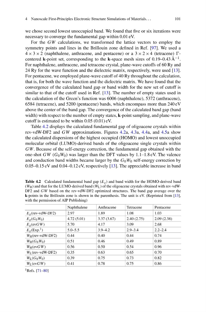
Table 4.2 displays the calculated fundamental gap of oligoacene crystals within
rev-vdW-DF2 and GW approximations. Figures 4.2a, 4.3a, 4.4a, and 4.5a show
the calculated dispersions of the highest occupied (HOMO) and lowest unoccupied
molecular orbital (LUMO)-derived bands of the oligoacene single crystals within
GW . Because of the self-energy correction, the fundamental gap obtained with the
one-shot GW (G 0 W 0 ) was larger than the DFT values by 1.1–1.8 eV. The valence
and conduction band widths became larger by the G 0 W 0 self-energy correction by
0.05–0.15 eV and 0.04–0.12 eV, respectively [13]. The appreciable increase in band
Table 4.2 Calculated fundamental band gap (E g ) and band width for the HOMO-derived band
(W H ) and that for the LUMO-derived band (W L ) of the oligoacene crystals obtained with rev-vdWDF2 and GW based on the rev-vdW-DF2 optimized structures. The band gap average over the
k-points in the Brillouin zone is shown in the parenthesis. The unit is eV. (Reprinted from [13],
with the permission of AIP Publishing)
Naphthalene
Anthracene
Tetracene
Pentacene
E g (rev-vdW-DF2)
2.97
1.89
1.08
1.03
E g (G 0 W 0 )
4.72 (5.01)
3.37 (3.67)
2.40 (2.75)
2.09 (2.38)
E g (evGW )
5.70
4.17
3.09
2.68
E g (Exp. 1 )
5.0–5.5
3.9–4.2
2.9–3.4
2.2–2.4
W H (rev-vdW-DF2)
0.44
0.40
0.44
0.74
W H (G 0 W 0 )
0.51
0.46
0.49
0.89
W H (evGW )
0.56
0.50
0.54
0.96
W L (rev-vdW-DF2)
0.35
0.63
0.65
0.70
W L (G 0 W 0 )
0.39
0.75
0.73
0.82
W L (evGW )
0.41
0.78
0.75
0.86
1 Refs. [71–80]
101
we chose second lowest unoccupied band. We found that five or six iterations were
necessary to converge the fundamental gap within 0.01 eV.
For the GW calculations, we transformed the lattice vectors to employ the
symmetry points and lines in the Brillouin zone defined in Ref. [97]. We used a
4 × 3 × 2 (naphthalene, anthracene, and pentacene) or a 3 × 2 × 4 (tetracene) -
centered k-point set, corresponding to the k-space mesh sizes of 0.19–0.43 Å −1 .
For naphthalene, anthracene, and tetracene crystal, plane-wave cutoffs of 60 Ry and
24 Ry for the wave function and the dielectric matrix, respectively, were used [13].
For pentacene, we employed plane-wave cutoff of 40 Ry throughout the calculation,
that is, for both the wave function and the dielectric matrix. We have found that the
convergence of the calculated band gap or band width for the new set of cutoff is
similar to that of the cutoff used in Ref. [13]. The number of empty states used in
the calculation of the Green’s function was 6006 (naphthalene), 5372 (anthracene),
6584 (tetracene), and 5200 (pentacene) bands, which encompass more than 240 eV
above the center of the band gap. The convergence of the calculated band gap (band
width) with respect to the number of empty states, k-point sampling, and plane-wave
cutoff is estimated to be within 0.05 (0.01) eV.
Table 4.2 displays the calculated fundamental gap of oligoacene crystals within
rev-vdW-DF2 and GW approximations. Figures 4.2a, 4.3a, 4.4a, and 4.5a show
the calculated dispersions of the highest occupied (HOMO) and lowest unoccupied
molecular orbital (LUMO)-derived bands of the oligoacene single crystals within
GW . Because of the self-energy correction, the fundamental gap obtained with the
one-shot GW (G 0 W 0 ) was larger than the DFT values by 1.1–1.8 eV. The valence
and conduction band widths became larger by the G 0 W 0 self-energy correction by
0.05–0.15 eV and 0.04–0.12 eV, respectively [13]. The appreciable increase in band
Table 4.2 Calculated fundamental band gap (E g ) and band width for the HOMO-derived band
(W H ) and that for the LUMO-derived band (W L ) of the oligoacene crystals obtained with rev-vdWDF2 and GW based on the rev-vdW-DF2 optimized structures. The band gap average over the
k-points in the Brillouin zone is shown in the parenthesis. The unit is eV. (Reprinted from [13],
with the permission of AIP Publishing)
Naphthalene
Anthracene
Tetracene
Pentacene
E g (rev-vdW-DF2)
2.97
1.89
1.08
1.03
E g (G 0 W 0 )
4.72 (5.01)
3.37 (3.67)
2.40 (2.75)
2.09 (2.38)
E g (evGW )
5.70
4.17
3.09
2.68
E g (Exp. 1 )
5.0–5.5
3.9–4.2
2.9–3.4
2.2–2.4
W H (rev-vdW-DF2)
0.44
0.40
0.44
0.74
W H (G 0 W 0 )
0.51
0.46
0.49
0.89
W H (evGW )
0.56
0.50
0.54
0.96
W L (rev-vdW-DF2)
0.35
0.63
0.65
0.70
W L (G 0 W 0 )
0.39
0.75
0.73
0.82
W L (evGW )
0.41
0.78
0.75
0.86
1 Refs. [71–80]