

86
4.
PHOTOELECTRIC EMISSION
cathode.
A positive space charge is thus built up in the crystal
and serves to retard the movement of the electrons so that the
photo-current decreases with continued exposure
to the light. The
existence of a positive space charge may be shown when the crystal
is mounted close to an elecLight
«»
-
trode connected to _the leaf of
»
an
electroscope.
Continued
J, 1 1
exposure
to
the light causes
CRYSTAL
_
METAL
the leaf to move in such a
ELECTRODE
.
.
..
direction as would be caused
AN0DE
///
/ /
by the accumulation of
_
a
.
,
// // Ï
positive charge. If the crystal
is exposed to infra—red rays
.
or
is heated, the positive
space
charge is decreased.
”
.
With this decrease
in
the
'
+
"' l'l
_
0
space charge, it is found that
_
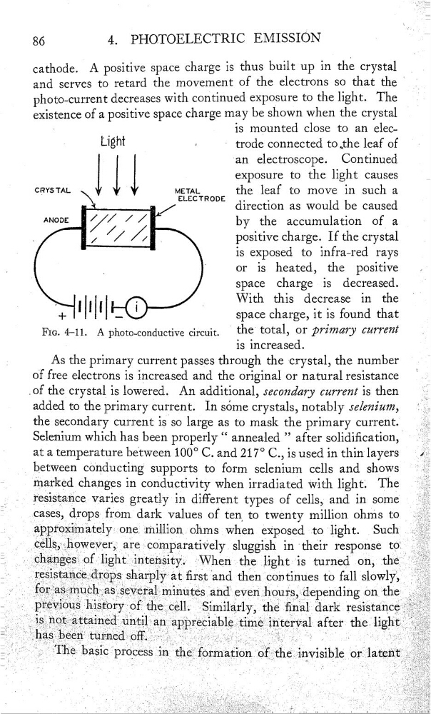
FIG. 4—11.
A photo-conductive circuit.
_
t0tal> or primary current
.
is increased.
As the primary current passes through the crystal, the number
of free electrons is increased and the original or natural resistance
of the crystal is lowered. An additional, secondary current is then
added to the primary current. In sème crystals, notably selenium,
the secondary current isso large as to mask the primary current.
Selenium which has been properly
“
annealed
”
after solidication, ‘
at a temperature between 100° C. and 217° C., is used in thinlayers
a
__
between
supports to form selenium cells and shows
marked changes in conductivity when irradiated With light. The
.
resistance, varies greatly in different types of cells, and in some
drops from dark values of
to twenty million ohms to
{million o”hms,when exposed to light.
Such
‘
cells,however, are _ comparatively sluggish in their response to'}
‘ changesoflightÎ
the light is turned on, the
resmtancedropssharplyat rst and then continues to fall siowly“,
prevmuShïst01‘Y0f’hêœll Sunriarly,the nal dark res1stance
ntttnduntlnppbltmntv1 after the hght
hasbeenturncdo£î
A
;
—
Ï’ Q‘ _ï'
The basic
Ÿ process in theformat10nofthe invisible orlatent
4.
PHOTOELECTRIC EMISSION
cathode.
A positive space charge is thus built up in the crystal
and serves to retard the movement of the electrons so that the
photo-current decreases with continued exposure
to the light. The
existence of a positive space charge may be shown when the crystal
is mounted close to an elecLight
«»
-
trode connected to _the leaf of
»
an
electroscope.
Continued
J, 1 1
exposure
to
the light causes
CRYSTAL
_
METAL
the leaf to move in such a
ELECTRODE
.
.
..
direction as would be caused
AN0DE
///
/ /
by the accumulation of
_
a
.
,
// // Ï
positive charge. If the crystal
is exposed to infra—red rays
.
or
is heated, the positive
space
charge is decreased.
”
.
With this decrease
in
the
'
+
"' l'l
_
0
space charge, it is found that
_
FIG. 4—11.
A photo-conductive circuit.
_
t0tal> or primary current
.
is increased.
As the primary current passes through the crystal, the number
of free electrons is increased and the original or natural resistance
of the crystal is lowered. An additional, secondary current is then
added to the primary current. In sème crystals, notably selenium,
the secondary current isso large as to mask the primary current.
Selenium which has been properly
“
annealed
”
after solidication, ‘
at a temperature between 100° C. and 217° C., is used in thinlayers
a
__
between
supports to form selenium cells and shows
marked changes in conductivity when irradiated With light. The
.
resistance, varies greatly in different types of cells, and in some
drops from dark values of
to twenty million ohms to
{million o”hms,when exposed to light.
Such
‘
cells,however, are _ comparatively sluggish in their response to'}
‘ changesoflightÎ
the light is turned on, the
resmtancedropssharplyat rst and then continues to fall siowly“,
prevmuShïst01‘Y0f’hêœll Sunriarly,the nal dark res1stance
ntttnduntlnppbltmntv1 after the hght
hasbeenturncdo£î
A
;
—
Ï’ Q‘ _ï'
The basic
Ÿ process in theformat10nofthe invisible orlatent