

454
S. V. Boriskina
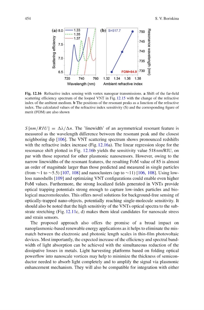
Fig. 12.16 Refractive index sensing with vortex nanogear transmissions. a Shift of the far-field
scattering efficiency spectrum of the looped VNT in Fig. 12.15 with the change of the refractive
index of the ambient medium. b The positions of the resonant peaks as a function of the refractive
index. The calculated values of the refractive index sensitivity (S) and the corresponding figure of
merit (FOM) are also shown
S [nm/R I U ] = δΔ/δn. The ’linewidth’ of an asymmetrical resonant feature is
measured as the wavelength difference between the resonant peak and the closest
neighboring dip [106]. The VNT scattering spectrum shows pronounced redshifts
with the refractive index increase (Fig. 12.16a). The linear regression slope for the
resonance shift plotted in Fig. 12.16b yields the sensitivity value 518 nm/RIU, on
par with those reported for other plasmonic nanosensors. However, owing to the
narrow linewidths of the resonant features, the resulting FoM value of 85 is almost
an order of magnitude larger than those predicted and measured in single particles
(from √1 to √5.5) [107, 108] and nanoclusters (up to √11) [106, 108]. Using lowloss nanoshells [109] and optimizing VNT configurations could enable even higher
FoM values. Furthermore, the strong localized fields generated in VNTs provide
optical trapping potentials strong enough to capture low-index particles and biological macromolecules. This offers novel solutions for background-free sensing of
optically-trapped nano-objects, potentially reaching single-molecule sensitivity. It
should also be noted that the high sensitivity of the VNTs optical spectra to the substrate stretching (Fig. 12.11c, d) makes them ideal candidates for nanoscale stress
and strain sensors.
The proposed approach also offers the promise of a broad impact on
nanoplasmonic-based renewable energy applications as it helps to eliminate the mismatch between the electronic and photonic length scales in thin-film photovoltaic
devices. Most importantly, the expected increase of the efficiency and spectral bandwidth of light absorption can be achieved with the simultaneous reduction of the
dissipative losses in metals. Light harvesting platforms based on folding optical
powerflow into nanoscale vortices may help to minimize the thickness of semiconductor needed to absorb light completely and to amplify the signal via plasmonic
enhancement mechanism. They will also be compatible for integration with either
S. V. Boriskina
Fig. 12.16 Refractive index sensing with vortex nanogear transmissions. a Shift of the far-field
scattering efficiency spectrum of the looped VNT in Fig. 12.15 with the change of the refractive
index of the ambient medium. b The positions of the resonant peaks as a function of the refractive
index. The calculated values of the refractive index sensitivity (S) and the corresponding figure of
merit (FOM) are also shown
S [nm/R I U ] = δΔ/δn. The ’linewidth’ of an asymmetrical resonant feature is
measured as the wavelength difference between the resonant peak and the closest
neighboring dip [106]. The VNT scattering spectrum shows pronounced redshifts
with the refractive index increase (Fig. 12.16a). The linear regression slope for the
resonance shift plotted in Fig. 12.16b yields the sensitivity value 518 nm/RIU, on
par with those reported for other plasmonic nanosensors. However, owing to the
narrow linewidths of the resonant features, the resulting FoM value of 85 is almost
an order of magnitude larger than those predicted and measured in single particles
(from √1 to √5.5) [107, 108] and nanoclusters (up to √11) [106, 108]. Using lowloss nanoshells [109] and optimizing VNT configurations could enable even higher
FoM values. Furthermore, the strong localized fields generated in VNTs provide
optical trapping potentials strong enough to capture low-index particles and biological macromolecules. This offers novel solutions for background-free sensing of
optically-trapped nano-objects, potentially reaching single-molecule sensitivity. It
should also be noted that the high sensitivity of the VNTs optical spectra to the substrate stretching (Fig. 12.11c, d) makes them ideal candidates for nanoscale stress
and strain sensors.
The proposed approach also offers the promise of a broad impact on
nanoplasmonic-based renewable energy applications as it helps to eliminate the mismatch between the electronic and photonic length scales in thin-film photovoltaic
devices. Most importantly, the expected increase of the efficiency and spectral bandwidth of light absorption can be achieved with the simultaneous reduction of the
dissipative losses in metals. Light harvesting platforms based on folding optical
powerflow into nanoscale vortices may help to minimize the thickness of semiconductor needed to absorb light completely and to amplify the signal via plasmonic
enhancement mechanism. They will also be compatible for integration with either