

452
S. V. Boriskina
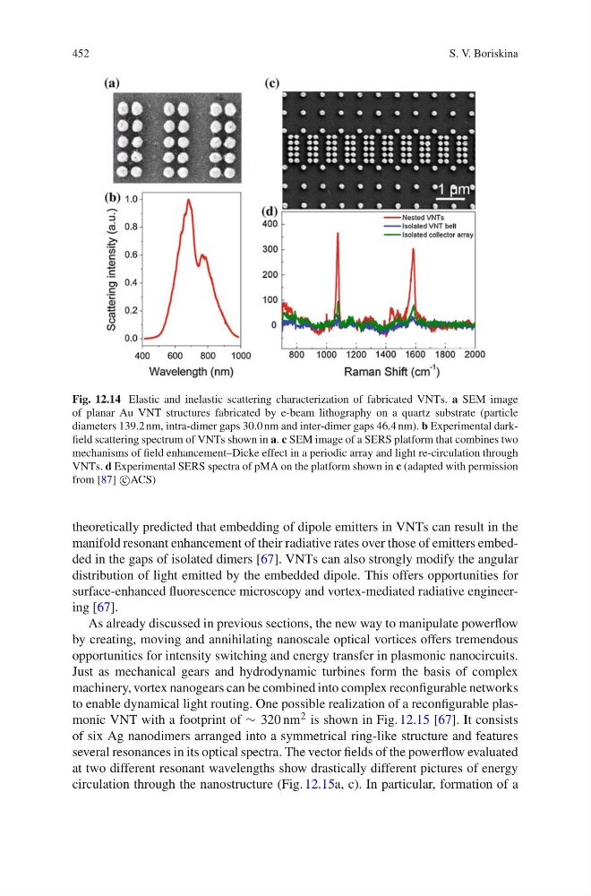
Fig. 12.14 Elastic and inelastic scattering characterization of fabricated VNTs. a SEM image
of planar Au VNT structures fabricated by e-beam lithography on a quartz substrate (particle
diameters 139.2 nm, intra-dimer gaps 30.0 nm and inter-dimer gaps 46.4 nm). b Experimental darkfield scattering spectrum of VNTs shown in a. c SEM image of a SERS platform that combines two
mechanisms of field enhancement–Dicke effect in a periodic array and light re-circulation through
VNTs. d Experimental SERS spectra of pMA on the platform shown in c (adapted with permission
from [87] c
∪ACS)
theoretically predicted that embedding of dipole emitters in VNTs can result in the
manifold resonant enhancement of their radiative rates over those of emitters embedded in the gaps of isolated dimers [67]. VNTs can also strongly modify the angular
distribution of light emitted by the embedded dipole. This offers opportunities for
surface-enhanced fluorescence microscopy and vortex-mediated radiative engineering [67].
As already discussed in previous sections, the new way to manipulate powerflow
by creating, moving and annihilating nanoscale optical vortices offers tremendous
opportunities for intensity switching and energy transfer in plasmonic nanocircuits.
Just as mechanical gears and hydrodynamic turbines form the basis of complex
machinery, vortex nanogears can be combined into complex reconfigurable networks
to enable dynamical light routing. One possible realization of a reconfigurable plasmonic VNT with a footprint of √ 320 nm 2 is shown in Fig. 12.15 [67]. It consists
of six Ag nanodimers arranged into a symmetrical ring-like structure and features
several resonances in its optical spectra. The vector fields of the powerflow evaluated
at two different resonant wavelengths show drastically different pictures of energy
circulation through the nanostructure (Fig. 12.15a, c). In particular, formation of a
S. V. Boriskina
Fig. 12.14 Elastic and inelastic scattering characterization of fabricated VNTs. a SEM image
of planar Au VNT structures fabricated by e-beam lithography on a quartz substrate (particle
diameters 139.2 nm, intra-dimer gaps 30.0 nm and inter-dimer gaps 46.4 nm). b Experimental darkfield scattering spectrum of VNTs shown in a. c SEM image of a SERS platform that combines two
mechanisms of field enhancement–Dicke effect in a periodic array and light re-circulation through
VNTs. d Experimental SERS spectra of pMA on the platform shown in c (adapted with permission
from [87] c
∪ACS)
theoretically predicted that embedding of dipole emitters in VNTs can result in the
manifold resonant enhancement of their radiative rates over those of emitters embedded in the gaps of isolated dimers [67]. VNTs can also strongly modify the angular
distribution of light emitted by the embedded dipole. This offers opportunities for
surface-enhanced fluorescence microscopy and vortex-mediated radiative engineering [67].
As already discussed in previous sections, the new way to manipulate powerflow
by creating, moving and annihilating nanoscale optical vortices offers tremendous
opportunities for intensity switching and energy transfer in plasmonic nanocircuits.
Just as mechanical gears and hydrodynamic turbines form the basis of complex
machinery, vortex nanogears can be combined into complex reconfigurable networks
to enable dynamical light routing. One possible realization of a reconfigurable plasmonic VNT with a footprint of √ 320 nm 2 is shown in Fig. 12.15 [67]. It consists
of six Ag nanodimers arranged into a symmetrical ring-like structure and features
several resonances in its optical spectra. The vector fields of the powerflow evaluated
at two different resonant wavelengths show drastically different pictures of energy
circulation through the nanostructure (Fig. 12.15a, c). In particular, formation of a