

4 Silicon Plasmonics
161
A different geometry was developed by our group at the Hebrew University [51].
Our approach is based on a self-aligned fabrication approach of local-oxidation of
silicon (LOCOS) on SOI substrate, where nanoscale waveguide structure is defined
by oxide spacers. Implementation of the LOCOS process provides compatibility
with standard CMOS technology and permits a precise control over the shape and
the dimensions of the waveguide [4]. Additionally, the LOCOS technique enables
the fabrication of low-loss bus photonic waveguide (ca. 0.3 dB/cm) and the detector
in the same process step, where the oxide spacers effectively define the area of metalsilicon interface and thus allow avoiding lateral misalignment between the silicon
surface and the metal layer to form a Schottky contact.
Our device was fabricated by depositing a 100 nm of silicon nitride (SiN) on top
of a 340 nm-thick, silicon device layer which is separated from the handle wafer
by a 2 μm-thick buried oxide. Next, the mask defining the optical and electrical
structures including the photonic bus waveguide, the detection region and the contacts area were patterned into the protective SiN layer using standard electron-beam
lithography (EBL) followed by reactive ion etching (RIE). The defined pattern was
next transferred to the silicon layer by wet oxidation process where the nitride layer
serves as a mask preventing the oxygen diffusion. After oxidation the nitride mask
was removed by an additional RIE step. To make the Schottky plasmonic photodetector we firstly realized an ohmic contact to the silicon layer by evaporating an
aluminum pad and alloying the structure at 450 ◦ C. Finally, a 50 nm-thick Au layer
was deposited onto the chip followed by a lift-off process to lay down the metallic
strip of the plasmonic structure to form a Schottky contact.
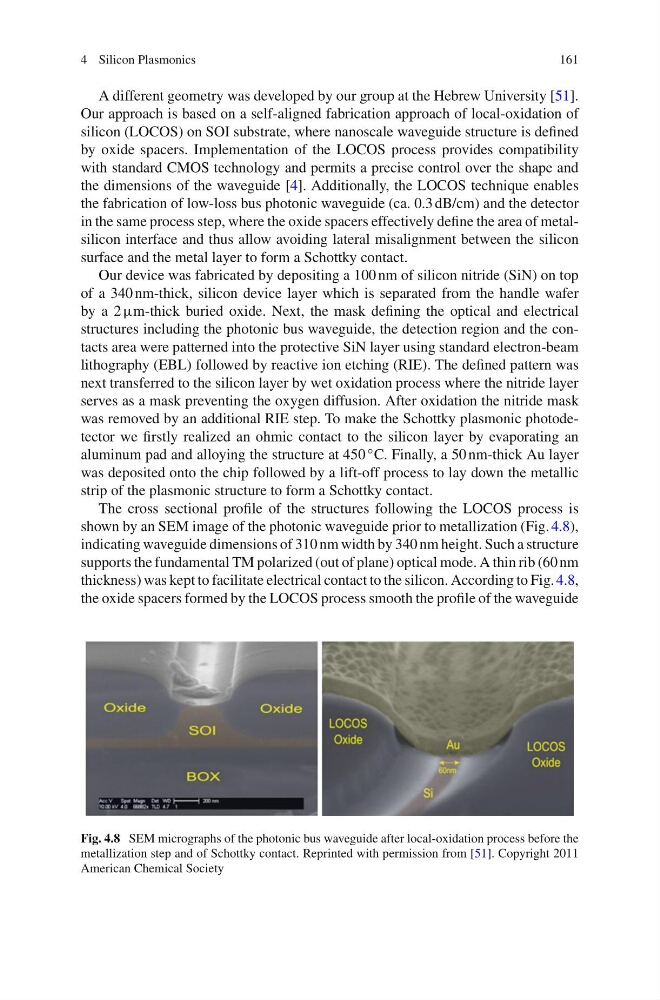
The cross sectional profile of the structures following the LOCOS process is
shown by an SEM image of the photonic waveguide prior to metallization (Fig. 4.8),
indicating waveguide dimensions of 310 nm width by 340 nm height. Such a structure
supports the fundamental TM polarized (out of plane) optical mode. A thin rib (60 nm
thickness) was kept to facilitate electrical contact to the silicon. According to Fig. 4.8,
the oxide spacers formed by the LOCOS process smooth the profile of the waveguide
Fig. 4.8 SEM micrographs of the photonic bus waveguide after local-oxidation process before the
metallization step and of Schottky contact. Reprinted with permission from [51]. Copyright 2011
American Chemical Society
161
A different geometry was developed by our group at the Hebrew University [51].
Our approach is based on a self-aligned fabrication approach of local-oxidation of
silicon (LOCOS) on SOI substrate, where nanoscale waveguide structure is defined
by oxide spacers. Implementation of the LOCOS process provides compatibility
with standard CMOS technology and permits a precise control over the shape and
the dimensions of the waveguide [4]. Additionally, the LOCOS technique enables
the fabrication of low-loss bus photonic waveguide (ca. 0.3 dB/cm) and the detector
in the same process step, where the oxide spacers effectively define the area of metalsilicon interface and thus allow avoiding lateral misalignment between the silicon
surface and the metal layer to form a Schottky contact.
Our device was fabricated by depositing a 100 nm of silicon nitride (SiN) on top
of a 340 nm-thick, silicon device layer which is separated from the handle wafer
by a 2 μm-thick buried oxide. Next, the mask defining the optical and electrical
structures including the photonic bus waveguide, the detection region and the contacts area were patterned into the protective SiN layer using standard electron-beam
lithography (EBL) followed by reactive ion etching (RIE). The defined pattern was
next transferred to the silicon layer by wet oxidation process where the nitride layer
serves as a mask preventing the oxygen diffusion. After oxidation the nitride mask
was removed by an additional RIE step. To make the Schottky plasmonic photodetector we firstly realized an ohmic contact to the silicon layer by evaporating an
aluminum pad and alloying the structure at 450 ◦ C. Finally, a 50 nm-thick Au layer
was deposited onto the chip followed by a lift-off process to lay down the metallic
strip of the plasmonic structure to form a Schottky contact.
The cross sectional profile of the structures following the LOCOS process is
shown by an SEM image of the photonic waveguide prior to metallization (Fig. 4.8),
indicating waveguide dimensions of 310 nm width by 340 nm height. Such a structure
supports the fundamental TM polarized (out of plane) optical mode. A thin rib (60 nm
thickness) was kept to facilitate electrical contact to the silicon. According to Fig. 4.8,
the oxide spacers formed by the LOCOS process smooth the profile of the waveguide
Fig. 4.8 SEM micrographs of the photonic bus waveguide after local-oxidation process before the
metallization step and of Schottky contact. Reprinted with permission from [51]. Copyright 2011
American Chemical Society