

162
I. Goykhman et al.
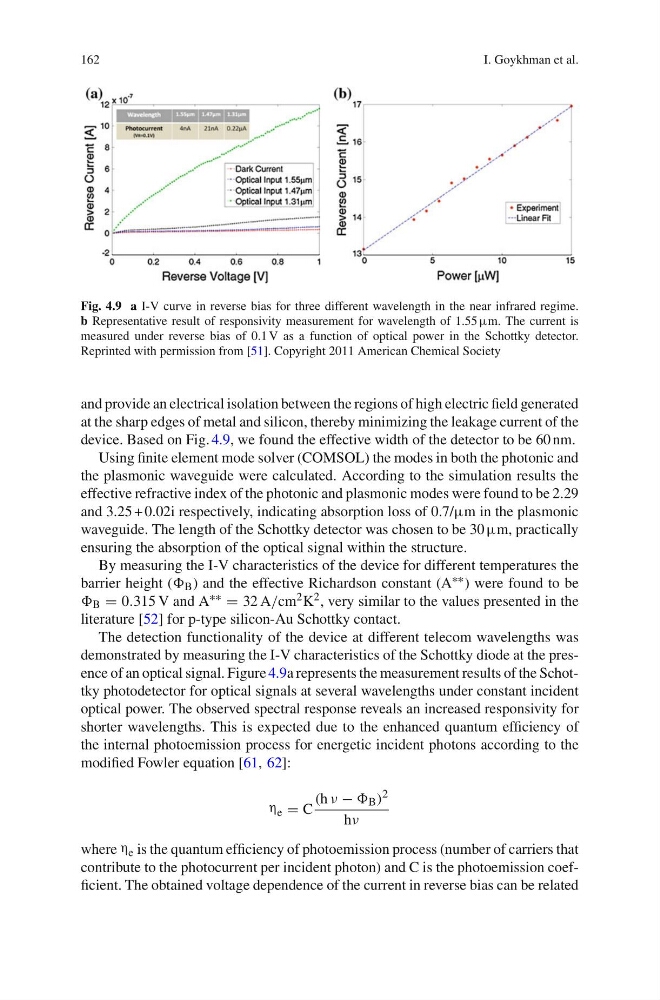
Fig. 4.9 a I-V curve in reverse bias for three different wavelength in the near infrared regime.
b Representative result of responsivity measurement for wavelength of 1.55 μm. The current is
measured under reverse bias of 0.1 V as a function of optical power in the Schottky detector.
Reprinted with permission from [51]. Copyright 2011 American Chemical Society
and provide an electrical isolation between the regions of high electric field generated
at the sharp edges of metal and silicon, thereby minimizing the leakage current of the
device. Based on Fig. 4.9, we found the effective width of the detector to be 60 nm.
Using finite element mode solver (COMSOL) the modes in both the photonic and
the plasmonic waveguide were calculated. According to the simulation results the
effective refractive index of the photonic and plasmonic modes were found to be 2.29
and 3.25 + 0.02i respectively, indicating absorption loss of 0.7/μm in the plasmonic
waveguide. The length of the Schottky detector was chosen to be 30 μm, practically
ensuring the absorption of the optical signal within the structure.
By measuring the I-V characteristics of the device for different temperatures the
barrier height (ε B ) and the effective Richardson constant (A ∗∗ ) were found to be
ε B = 0.315 V and A ∗∗ = 32 A/cm 2 K 2 , very similar to the values presented in the
literature [52] for p-type silicon-Au Schottky contact.
The detection functionality of the device at different telecom wavelengths was
demonstrated by measuring the I-V characteristics of the Schottky diode at the presence of an optical signal. Figure 4.9a represents the measurement results of the Schottky photodetector for optical signals at several wavelengths under constant incident
optical power. The observed spectral response reveals an increased responsivity for
shorter wavelengths. This is expected due to the enhanced quantum efficiency of
the internal photoemission process for energetic incident photons according to the
modified Fowler equation [61, 62]:
η e = C
(h λ − ε B )
2
hλ
where η e is the quantum efficiency of photoemission process (number of carriers that
contribute to the photocurrent per incident photon) and C is the photoemission coefficient. The obtained voltage dependence of the current in reverse bias can be related
I. Goykhman et al.
Fig. 4.9 a I-V curve in reverse bias for three different wavelength in the near infrared regime.
b Representative result of responsivity measurement for wavelength of 1.55 μm. The current is
measured under reverse bias of 0.1 V as a function of optical power in the Schottky detector.
Reprinted with permission from [51]. Copyright 2011 American Chemical Society
and provide an electrical isolation between the regions of high electric field generated
at the sharp edges of metal and silicon, thereby minimizing the leakage current of the
device. Based on Fig. 4.9, we found the effective width of the detector to be 60 nm.
Using finite element mode solver (COMSOL) the modes in both the photonic and
the plasmonic waveguide were calculated. According to the simulation results the
effective refractive index of the photonic and plasmonic modes were found to be 2.29
and 3.25 + 0.02i respectively, indicating absorption loss of 0.7/μm in the plasmonic
waveguide. The length of the Schottky detector was chosen to be 30 μm, practically
ensuring the absorption of the optical signal within the structure.
By measuring the I-V characteristics of the device for different temperatures the
barrier height (ε B ) and the effective Richardson constant (A ∗∗ ) were found to be
ε B = 0.315 V and A ∗∗ = 32 A/cm 2 K 2 , very similar to the values presented in the
literature [52] for p-type silicon-Au Schottky contact.
The detection functionality of the device at different telecom wavelengths was
demonstrated by measuring the I-V characteristics of the Schottky diode at the presence of an optical signal. Figure 4.9a represents the measurement results of the Schottky photodetector for optical signals at several wavelengths under constant incident
optical power. The observed spectral response reveals an increased responsivity for
shorter wavelengths. This is expected due to the enhanced quantum efficiency of
the internal photoemission process for energetic incident photons according to the
modified Fowler equation [61, 62]:
η e = C
(h λ − ε B )
2
hλ
where η e is the quantum efficiency of photoemission process (number of carriers that
contribute to the photocurrent per incident photon) and C is the photoemission coefficient. The obtained voltage dependence of the current in reverse bias can be related