

160
I. Goykhman et al.
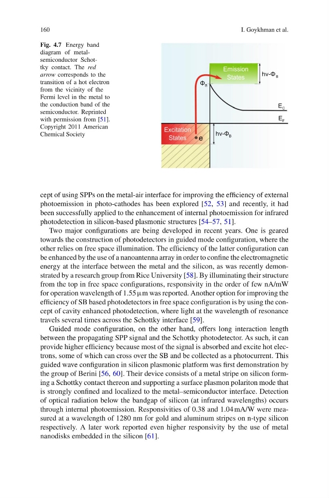
Fig. 4.7 Energy band
diagram of metalsemiconductor Schottky contact. The red
arrow corresponds to the
transition of a hot electron
from the vicinity of the
Fermi level in the metal to
the conduction band of the
semiconductor. Reprinted
with permission from [51].
Copyright 2011 American
Chemical Society
B
h -
B
C
E
F
E
B
h -
cept of using SPPs on the metal-air interface for improving the efficiency of external
photoemission in photo-cathodes has been explored [52, 53] and recently, it had
been successfully applied to the enhancement of internal photoemission for infrared
photodetection in silicon-based plasmonic structures [54–57, 51].
Two major configurations are being developed in recent years. One is geared
towards the construction of photodetectors in guided mode configuration, where the
other relies on free space illumination. The efficiency of the latter configuration can
be enhanced by the use of a nanoantenna array in order to confine the electromagnetic
energy at the interface between the metal and the silicon, as was recently demonstrated by a research group from Rice University [58]. By illuminating their structure
from the top in free space configurations, responsivity in the order of few nA/mW
for operation wavelength of 1.55 μm was reported. Another option for improving the
efficiency of SB based photodetectors in free space configuration is by using the concept of cavity enhanced photodetection, where light at the wavelength of resonance
travels several times across the Schottky interface [59].
Guided mode configuration, on the other hand, offers long interaction length
between the propagating SPP signal and the Schottky photodetector. As such, it can
provide higher efficiency because most of the signal is absorbed and excite hot electrons, some of which can cross over the SB and be collected as a photocurrent. This
guided wave configuration in silicon plasmonic platform was first demonstration by
the group of Berini [56, 60]. Their device consists of a metal stripe on silicon forming a Schottky contact thereon and supporting a surface plasmon polariton mode that
is strongly confined and localized to the metal–semiconductor interface. Detection
of optical radiation below the bandgap of silicon (at infrared wavelengths) occurs
through internal photoemission. Responsivities of 0.38 and 1.04 mA/W were measured at a wavelength of 1280 nm for gold and aluminum stripes on n-type silicon
respectively. A later work reported even higher responsivity by the use of metal
nanodisks embedded in the silicon [61].
I. Goykhman et al.
Fig. 4.7 Energy band
diagram of metalsemiconductor Schottky contact. The red
arrow corresponds to the
transition of a hot electron
from the vicinity of the
Fermi level in the metal to
the conduction band of the
semiconductor. Reprinted
with permission from [51].
Copyright 2011 American
Chemical Society
B
h -
B
C
E
F
E
B
h -
cept of using SPPs on the metal-air interface for improving the efficiency of external
photoemission in photo-cathodes has been explored [52, 53] and recently, it had
been successfully applied to the enhancement of internal photoemission for infrared
photodetection in silicon-based plasmonic structures [54–57, 51].
Two major configurations are being developed in recent years. One is geared
towards the construction of photodetectors in guided mode configuration, where the
other relies on free space illumination. The efficiency of the latter configuration can
be enhanced by the use of a nanoantenna array in order to confine the electromagnetic
energy at the interface between the metal and the silicon, as was recently demonstrated by a research group from Rice University [58]. By illuminating their structure
from the top in free space configurations, responsivity in the order of few nA/mW
for operation wavelength of 1.55 μm was reported. Another option for improving the
efficiency of SB based photodetectors in free space configuration is by using the concept of cavity enhanced photodetection, where light at the wavelength of resonance
travels several times across the Schottky interface [59].
Guided mode configuration, on the other hand, offers long interaction length
between the propagating SPP signal and the Schottky photodetector. As such, it can
provide higher efficiency because most of the signal is absorbed and excite hot electrons, some of which can cross over the SB and be collected as a photocurrent. This
guided wave configuration in silicon plasmonic platform was first demonstration by
the group of Berini [56, 60]. Their device consists of a metal stripe on silicon forming a Schottky contact thereon and supporting a surface plasmon polariton mode that
is strongly confined and localized to the metal–semiconductor interface. Detection
of optical radiation below the bandgap of silicon (at infrared wavelengths) occurs
through internal photoemission. Responsivities of 0.38 and 1.04 mA/W were measured at a wavelength of 1280 nm for gold and aluminum stripes on n-type silicon
respectively. A later work reported even higher responsivity by the use of metal
nanodisks embedded in the silicon [61].