

156
I. Goykhman et al.
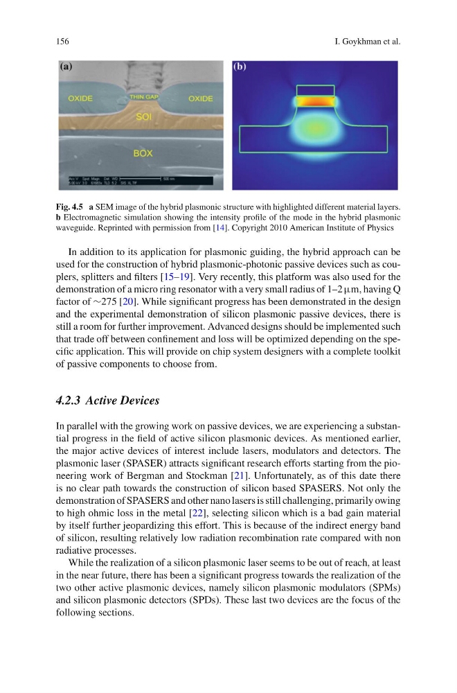
Fig. 4.5 a SEM image of the hybrid plasmonic structure with highlighted different material layers.
b Electromagnetic simulation showing the intensity profile of the mode in the hybrid plasmonic
waveguide. Reprinted with permission from [14]. Copyright 2010 American Institute of Physics
In addition to its application for plasmonic guiding, the hybrid approach can be
used for the construction of hybrid plasmonic-photonic passive devices such as couplers, splitters and filters [15–19]. Very recently, this platform was also used for the
demonstration of a micro ring resonator with a very small radius of 1–2 μm, having Q
factor of ∼275 [20]. While significant progress has been demonstrated in the design
and the experimental demonstration of silicon plasmonic passive devices, there is
still a room for further improvement. Advanced designs should be implemented such
that trade off between confinement and loss will be optimized depending on the specific application. This will provide on chip system designers with a complete toolkit
of passive components to choose from.
4.2.3 Active Devices
In parallel with the growing work on passive devices, we are experiencing a substantial progress in the field of active silicon plasmonic devices. As mentioned earlier,
the major active devices of interest include lasers, modulators and detectors. The
plasmonic laser (SPASER) attracts significant research efforts starting from the pioneering work of Bergman and Stockman [21]. Unfortunately, as of this date there
is no clear path towards the construction of silicon based SPASERS. Not only the
demonstration of SPASERS and other nano lasers is still challenging, primarily owing
to high ohmic loss in the metal [22], selecting silicon which is a bad gain material
by itself further jeopardizing this effort. This is because of the indirect energy band
of silicon, resulting relatively low radiation recombination rate compared with non
radiative processes.
While the realization of a silicon plasmonic laser seems to be out of reach, at least
in the near future, there has been a significant progress towards the realization of the
two other active plasmonic devices, namely silicon plasmonic modulators (SPMs)
and silicon plasmonic detectors (SPDs). These last two devices are the focus of the
following sections.
I. Goykhman et al.
Fig. 4.5 a SEM image of the hybrid plasmonic structure with highlighted different material layers.
b Electromagnetic simulation showing the intensity profile of the mode in the hybrid plasmonic
waveguide. Reprinted with permission from [14]. Copyright 2010 American Institute of Physics
In addition to its application for plasmonic guiding, the hybrid approach can be
used for the construction of hybrid plasmonic-photonic passive devices such as couplers, splitters and filters [15–19]. Very recently, this platform was also used for the
demonstration of a micro ring resonator with a very small radius of 1–2 μm, having Q
factor of ∼275 [20]. While significant progress has been demonstrated in the design
and the experimental demonstration of silicon plasmonic passive devices, there is
still a room for further improvement. Advanced designs should be implemented such
that trade off between confinement and loss will be optimized depending on the specific application. This will provide on chip system designers with a complete toolkit
of passive components to choose from.
4.2.3 Active Devices
In parallel with the growing work on passive devices, we are experiencing a substantial progress in the field of active silicon plasmonic devices. As mentioned earlier,
the major active devices of interest include lasers, modulators and detectors. The
plasmonic laser (SPASER) attracts significant research efforts starting from the pioneering work of Bergman and Stockman [21]. Unfortunately, as of this date there
is no clear path towards the construction of silicon based SPASERS. Not only the
demonstration of SPASERS and other nano lasers is still challenging, primarily owing
to high ohmic loss in the metal [22], selecting silicon which is a bad gain material
by itself further jeopardizing this effort. This is because of the indirect energy band
of silicon, resulting relatively low radiation recombination rate compared with non
radiative processes.
While the realization of a silicon plasmonic laser seems to be out of reach, at least
in the near future, there has been a significant progress towards the realization of the
two other active plasmonic devices, namely silicon plasmonic modulators (SPMs)
and silicon plasmonic detectors (SPDs). These last two devices are the focus of the
following sections.