

4 Silicon Plasmonics
155
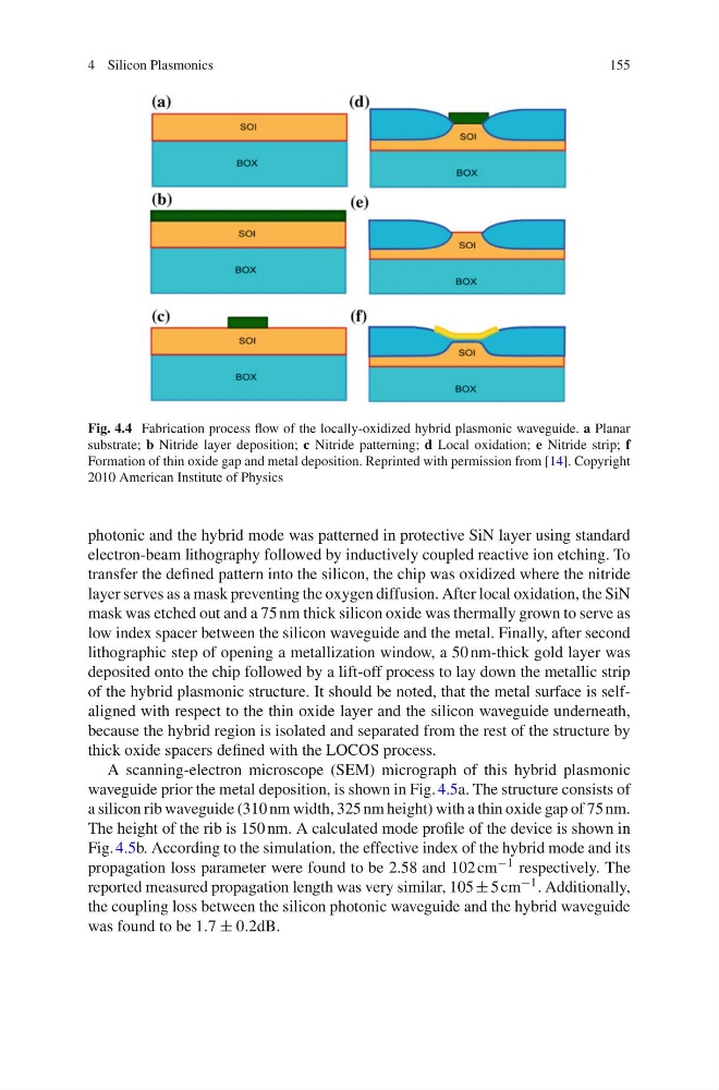
Fig. 4.4 Fabrication process flow of the locally-oxidized hybrid plasmonic waveguide. a Planar
substrate; b Nitride layer deposition; c Nitride patterning; d Local oxidation; e Nitride strip; f
Formation of thin oxide gap and metal deposition. Reprinted with permission from [14]. Copyright
2010 American Institute of Physics
photonic and the hybrid mode was patterned in protective SiN layer using standard
electron-beam lithography followed by inductively coupled reactive ion etching. To
transfer the defined pattern into the silicon, the chip was oxidized where the nitride
layer serves as a mask preventing the oxygen diffusion. After local oxidation, the SiN
mask was etched out and a 75 nm thick silicon oxide was thermally grown to serve as
low index spacer between the silicon waveguide and the metal. Finally, after second
lithographic step of opening a metallization window, a 50 nm-thick gold layer was
deposited onto the chip followed by a lift-off process to lay down the metallic strip
of the hybrid plasmonic structure. It should be noted, that the metal surface is selfaligned with respect to the thin oxide layer and the silicon waveguide underneath,
because the hybrid region is isolated and separated from the rest of the structure by
thick oxide spacers defined with the LOCOS process.
A scanning-electron microscope (SEM) micrograph of this hybrid plasmonic
waveguide prior the metal deposition, is shown in Fig. 4.5a. The structure consists of
a silicon rib waveguide (310 nm width, 325 nm height) with a thin oxide gap of 75 nm.
The height of the rib is 150 nm. A calculated mode profile of the device is shown in
Fig. 4.5b. According to the simulation, the effective index of the hybrid mode and its
propagation loss parameter were found to be 2.58 and 102 cm −1 respectively. The
reported measured propagation length was very similar, 105 ± 5 cm −1 . Additionally,
the coupling loss between the silicon photonic waveguide and the hybrid waveguide
was found to be 1.7 ± 0.2dB.
155
Fig. 4.4 Fabrication process flow of the locally-oxidized hybrid plasmonic waveguide. a Planar
substrate; b Nitride layer deposition; c Nitride patterning; d Local oxidation; e Nitride strip; f
Formation of thin oxide gap and metal deposition. Reprinted with permission from [14]. Copyright
2010 American Institute of Physics
photonic and the hybrid mode was patterned in protective SiN layer using standard
electron-beam lithography followed by inductively coupled reactive ion etching. To
transfer the defined pattern into the silicon, the chip was oxidized where the nitride
layer serves as a mask preventing the oxygen diffusion. After local oxidation, the SiN
mask was etched out and a 75 nm thick silicon oxide was thermally grown to serve as
low index spacer between the silicon waveguide and the metal. Finally, after second
lithographic step of opening a metallization window, a 50 nm-thick gold layer was
deposited onto the chip followed by a lift-off process to lay down the metallic strip
of the hybrid plasmonic structure. It should be noted, that the metal surface is selfaligned with respect to the thin oxide layer and the silicon waveguide underneath,
because the hybrid region is isolated and separated from the rest of the structure by
thick oxide spacers defined with the LOCOS process.
A scanning-electron microscope (SEM) micrograph of this hybrid plasmonic
waveguide prior the metal deposition, is shown in Fig. 4.5a. The structure consists of
a silicon rib waveguide (310 nm width, 325 nm height) with a thin oxide gap of 75 nm.
The height of the rib is 150 nm. A calculated mode profile of the device is shown in
Fig. 4.5b. According to the simulation, the effective index of the hybrid mode and its
propagation loss parameter were found to be 2.58 and 102 cm −1 respectively. The
reported measured propagation length was very similar, 105 ± 5 cm −1 . Additionally,
the coupling loss between the silicon photonic waveguide and the hybrid waveguide
was found to be 1.7 ± 0.2dB.