

154
I. Goykhman et al.
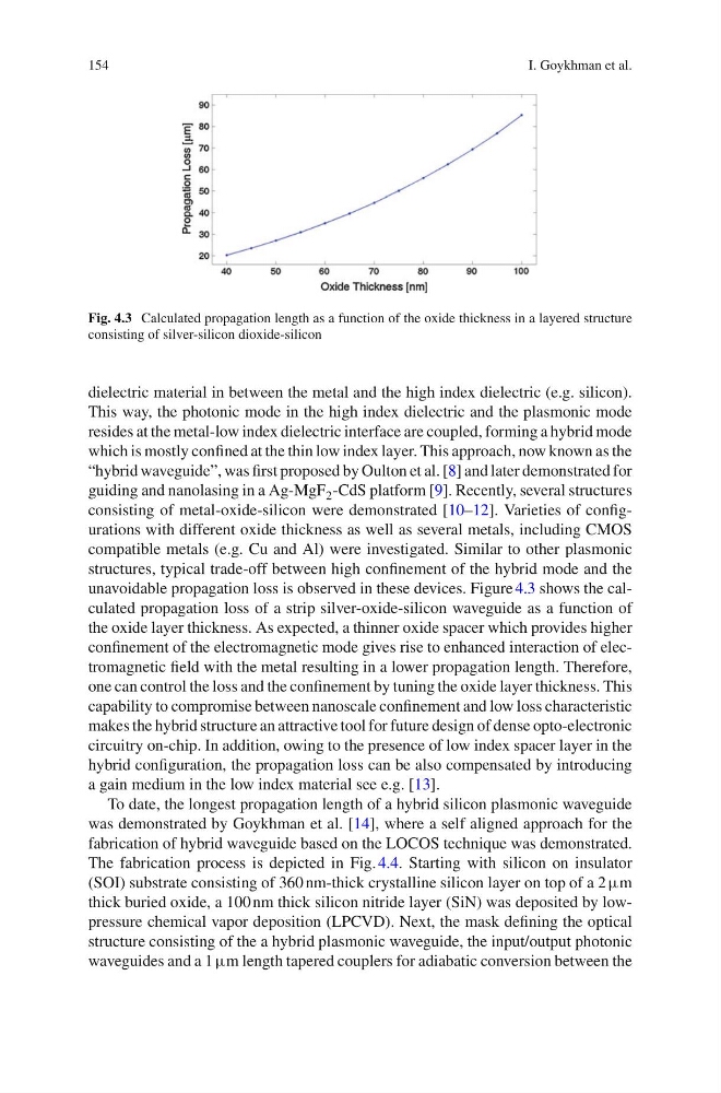
Fig. 4.3 Calculated propagation length as a function of the oxide thickness in a layered structure
consisting of silver-silicon dioxide-silicon
dielectric material in between the metal and the high index dielectric (e.g. silicon).
This way, the photonic mode in the high index dielectric and the plasmonic mode
resides at the metal-low index dielectric interface are coupled, forming a hybrid mode
which is mostly confined at the thin low index layer. This approach, now known as the
“hybrid waveguide”, was first proposed by Oulton et al. [8] and later demonstrated for
guiding and nanolasing in a Ag-MgF 2 -CdS platform [9]. Recently, several structures
consisting of metal-oxide-silicon were demonstrated [10–12]. Varieties of configurations with different oxide thickness as well as several metals, including CMOS
compatible metals (e.g. Cu and Al) were investigated. Similar to other plasmonic
structures, typical trade-off between high confinement of the hybrid mode and the
unavoidable propagation loss is observed in these devices. Figure 4.3 shows the calculated propagation loss of a strip silver-oxide-silicon waveguide as a function of
the oxide layer thickness. As expected, a thinner oxide spacer which provides higher
confinement of the electromagnetic mode gives rise to enhanced interaction of electromagnetic field with the metal resulting in a lower propagation length. Therefore,
one can control the loss and the confinement by tuning the oxide layer thickness. This
capability to compromise between nanoscale confinement and low loss characteristic
makes the hybrid structure an attractive tool for future design of dense opto-electronic
circuitry on-chip. In addition, owing to the presence of low index spacer layer in the
hybrid configuration, the propagation loss can be also compensated by introducing
a gain medium in the low index material see e.g. [13].
To date, the longest propagation length of a hybrid silicon plasmonic waveguide
was demonstrated by Goykhman et al. [14], where a self aligned approach for the
fabrication of hybrid waveguide based on the LOCOS technique was demonstrated.
The fabrication process is depicted in Fig. 4.4. Starting with silicon on insulator
(SOI) substrate consisting of 360 nm-thick crystalline silicon layer on top of a 2 μm
thick buried oxide, a 100 nm thick silicon nitride layer (SiN) was deposited by lowpressure chemical vapor deposition (LPCVD). Next, the mask defining the optical
structure consisting of the a hybrid plasmonic waveguide, the input/output photonic
waveguides and a 1 μm length tapered couplers for adiabatic conversion between the
I. Goykhman et al.
Fig. 4.3 Calculated propagation length as a function of the oxide thickness in a layered structure
consisting of silver-silicon dioxide-silicon
dielectric material in between the metal and the high index dielectric (e.g. silicon).
This way, the photonic mode in the high index dielectric and the plasmonic mode
resides at the metal-low index dielectric interface are coupled, forming a hybrid mode
which is mostly confined at the thin low index layer. This approach, now known as the
“hybrid waveguide”, was first proposed by Oulton et al. [8] and later demonstrated for
guiding and nanolasing in a Ag-MgF 2 -CdS platform [9]. Recently, several structures
consisting of metal-oxide-silicon were demonstrated [10–12]. Varieties of configurations with different oxide thickness as well as several metals, including CMOS
compatible metals (e.g. Cu and Al) were investigated. Similar to other plasmonic
structures, typical trade-off between high confinement of the hybrid mode and the
unavoidable propagation loss is observed in these devices. Figure 4.3 shows the calculated propagation loss of a strip silver-oxide-silicon waveguide as a function of
the oxide layer thickness. As expected, a thinner oxide spacer which provides higher
confinement of the electromagnetic mode gives rise to enhanced interaction of electromagnetic field with the metal resulting in a lower propagation length. Therefore,
one can control the loss and the confinement by tuning the oxide layer thickness. This
capability to compromise between nanoscale confinement and low loss characteristic
makes the hybrid structure an attractive tool for future design of dense opto-electronic
circuitry on-chip. In addition, owing to the presence of low index spacer layer in the
hybrid configuration, the propagation loss can be also compensated by introducing
a gain medium in the low index material see e.g. [13].
To date, the longest propagation length of a hybrid silicon plasmonic waveguide
was demonstrated by Goykhman et al. [14], where a self aligned approach for the
fabrication of hybrid waveguide based on the LOCOS technique was demonstrated.
The fabrication process is depicted in Fig. 4.4. Starting with silicon on insulator
(SOI) substrate consisting of 360 nm-thick crystalline silicon layer on top of a 2 μm
thick buried oxide, a 100 nm thick silicon nitride layer (SiN) was deposited by lowpressure chemical vapor deposition (LPCVD). Next, the mask defining the optical
structure consisting of the a hybrid plasmonic waveguide, the input/output photonic
waveguides and a 1 μm length tapered couplers for adiabatic conversion between the