

4 Silicon Plasmonics
153
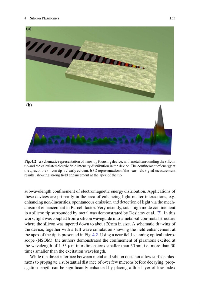
Fig. 4.2 a Schematic representation of nano-tip focusing device, with metal surrounding the silicon
tip and the calculated electric field intensity distribution in the device. The confinement of energy at
the apex of the silicon tip is clearly evident. b 3D representation of the near-field signal measurement
results, showing strong field enhancement at the apex of the tip
subwavelength confinement of electromagnetic energy distribution. Applications of
these devices are primarily in the area of enhancing light matter interactions, e.g.
enhancing non-linearities, spontaneous emission and detection of light via the mechanism of enhancement in Purcell factor. Very recently, such high mode confinement
in a silicon tip surrounded by metal was demonstrated by Desiatov et al. [7]. In this
work, light was coupled from a silicon waveguide into a metal-silicon-metal structure
where the silicon was tapered down to about 20 nm in size. A schematic drawing of
the device, together with a full wave simulation showing the field enhancement at
the apex of the tip is presented in Fig. 4.2. Using a near field scanning optical microscope (NSOM), the authors demonstrated the confinement of plasmons excited at
the wavelength of 1.55 μm into dimensions smaller than 50 nm, i.e. more than 30
times smaller than the excitation wavelength.
While the direct interface between metal and silicon does not allow surface plasmons to propagate a substantial distance of over few microns before decaying, propagation length can be significantly enhanced by placing a thin layer of low index
153
Fig. 4.2 a Schematic representation of nano-tip focusing device, with metal surrounding the silicon
tip and the calculated electric field intensity distribution in the device. The confinement of energy at
the apex of the silicon tip is clearly evident. b 3D representation of the near-field signal measurement
results, showing strong field enhancement at the apex of the tip
subwavelength confinement of electromagnetic energy distribution. Applications of
these devices are primarily in the area of enhancing light matter interactions, e.g.
enhancing non-linearities, spontaneous emission and detection of light via the mechanism of enhancement in Purcell factor. Very recently, such high mode confinement
in a silicon tip surrounded by metal was demonstrated by Desiatov et al. [7]. In this
work, light was coupled from a silicon waveguide into a metal-silicon-metal structure
where the silicon was tapered down to about 20 nm in size. A schematic drawing of
the device, together with a full wave simulation showing the field enhancement at
the apex of the tip is presented in Fig. 4.2. Using a near field scanning optical microscope (NSOM), the authors demonstrated the confinement of plasmons excited at
the wavelength of 1.55 μm into dimensions smaller than 50 nm, i.e. more than 30
times smaller than the excitation wavelength.
While the direct interface between metal and silicon does not allow surface plasmons to propagate a substantial distance of over few microns before decaying, propagation length can be significantly enhanced by placing a thin layer of low index