

152
I. Goykhman et al.
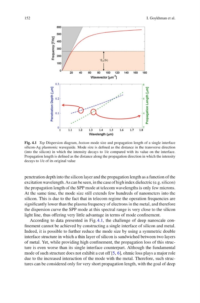
Fig. 4.1 Top Dispersion diagram, bottom mode size and propagation length of a single interface
silicon-Ag plasmonic waveguide. Mode size is defined as the distance in the transverse direction
(into the silicon) in which the intensity decays to 1/e compared with its value on the interface.
Propagation length is defined as the distance along the propagation direction in which the intensity
decays to 1/e of its original value
penetration depth into the silicon layer and the propagation length as a function of the
excitation wavelength. As can be seen, in the case of high index dielectric (e.g. silicon)
the propagation length of the SPP mode at telecom wavelengths is only few microns.
At the same time, the mode size still extends few hundreds of nanometers into the
silicon. This is due to the fact that in telecom regime the operation frequencies are
significantly lower than the plasma frequency of electrons in the metal, and therefore
the dispersion curve the SPP mode at this spectral range is very close to the silicon
light line, thus offering very little advantage in terms of mode confinement.
According to data presented in Fig. 4.1, the challenge of deep nanoscale confinement cannot be achieved by constructing a single interface of silicon and metal.
Indeed, it is possible to further reduce the mode size by using a symmetric double
interface structure in which a thin layer of silicon is sandwiched between two layers
of metal. Yet, while providing high confinement, the propagation loss of this structure is even worse than its single interface counterpart. Although the fundamental
mode of such structure does not exhibit a cut off [5, 6], ohmic loss plays a major role
due to the increased interaction of the mode with the metal. Therefore, such structures can be considered only for very short propagation length, with the goal of deep
I. Goykhman et al.
Fig. 4.1 Top Dispersion diagram, bottom mode size and propagation length of a single interface
silicon-Ag plasmonic waveguide. Mode size is defined as the distance in the transverse direction
(into the silicon) in which the intensity decays to 1/e compared with its value on the interface.
Propagation length is defined as the distance along the propagation direction in which the intensity
decays to 1/e of its original value
penetration depth into the silicon layer and the propagation length as a function of the
excitation wavelength. As can be seen, in the case of high index dielectric (e.g. silicon)
the propagation length of the SPP mode at telecom wavelengths is only few microns.
At the same time, the mode size still extends few hundreds of nanometers into the
silicon. This is due to the fact that in telecom regime the operation frequencies are
significantly lower than the plasma frequency of electrons in the metal, and therefore
the dispersion curve the SPP mode at this spectral range is very close to the silicon
light line, thus offering very little advantage in terms of mode confinement.
According to data presented in Fig. 4.1, the challenge of deep nanoscale confinement cannot be achieved by constructing a single interface of silicon and metal.
Indeed, it is possible to further reduce the mode size by using a symmetric double
interface structure in which a thin layer of silicon is sandwiched between two layers
of metal. Yet, while providing high confinement, the propagation loss of this structure is even worse than its single interface counterpart. Although the fundamental
mode of such structure does not exhibit a cut off [5, 6], ohmic loss plays a major role
due to the increased interaction of the mode with the metal. Therefore, such structures can be considered only for very short propagation length, with the goal of deep