

4 Silicon Plasmonics
157
4.2.3.1 Silicon Plasmonic Modulators
Similarly to their silicon photonics counterparts, advanced SPMs need to satisfy a
long list of features, such as low power consumption (typically measured as energy
per bit), high rate, high extinction ratio, relatively low loss, small foot print, linear
transfer function and more. However, unlike silicon photonic modulators, where
the required phase modulation can be achieved over a long propagation distance
(typically few millimeters, [23–26]), or alternatively via the use of resonators with
decent Q factors [27–32], the SPMs cannot rely on accumulating phase over a large
distances owing to the large propagation loss of the optical signals. Moreover, to
support on chip communication functionalities, the foot print of such SPMs should
not go beyond few microns.
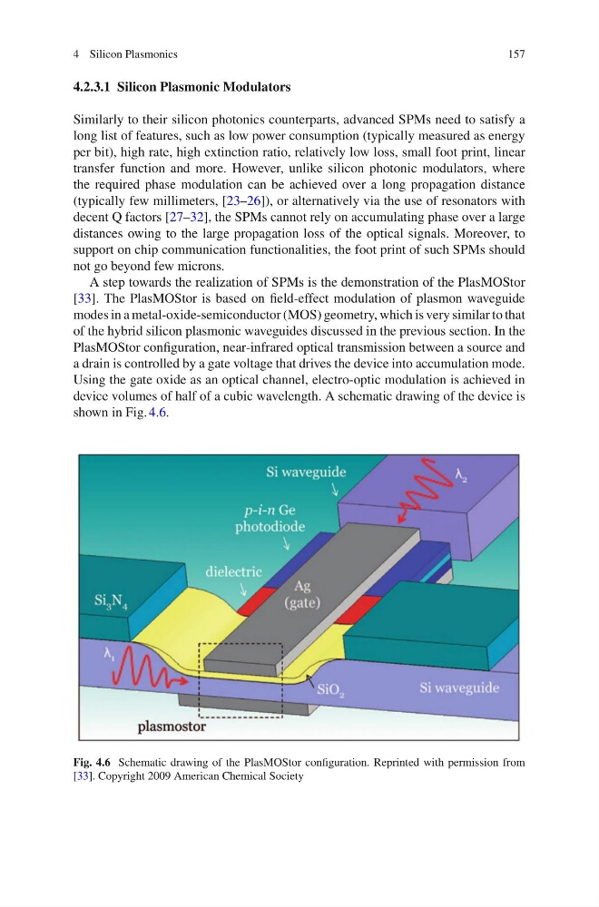
A step towards the realization of SPMs is the demonstration of the PlasMOStor
[33]. The PlasMOStor is based on field-effect modulation of plasmon waveguide
modes in a metal-oxide-semiconductor (MOS) geometry, which is very similar to that
of the hybrid silicon plasmonic waveguides discussed in the previous section. In the
PlasMOStor configuration, near-infrared optical transmission between a source and
a drain is controlled by a gate voltage that drives the device into accumulation mode.
Using the gate oxide as an optical channel, electro-optic modulation is achieved in
device volumes of half of a cubic wavelength. A schematic drawing of the device is
shown in Fig. 4.6.
Fig. 4.6 Schematic drawing of the PlasMOStor configuration. Reprinted with permission from
[33]. Copyright 2009 American Chemical Society
157
4.2.3.1 Silicon Plasmonic Modulators
Similarly to their silicon photonics counterparts, advanced SPMs need to satisfy a
long list of features, such as low power consumption (typically measured as energy
per bit), high rate, high extinction ratio, relatively low loss, small foot print, linear
transfer function and more. However, unlike silicon photonic modulators, where
the required phase modulation can be achieved over a long propagation distance
(typically few millimeters, [23–26]), or alternatively via the use of resonators with
decent Q factors [27–32], the SPMs cannot rely on accumulating phase over a large
distances owing to the large propagation loss of the optical signals. Moreover, to
support on chip communication functionalities, the foot print of such SPMs should
not go beyond few microns.
A step towards the realization of SPMs is the demonstration of the PlasMOStor
[33]. The PlasMOStor is based on field-effect modulation of plasmon waveguide
modes in a metal-oxide-semiconductor (MOS) geometry, which is very similar to that
of the hybrid silicon plasmonic waveguides discussed in the previous section. In the
PlasMOStor configuration, near-infrared optical transmission between a source and
a drain is controlled by a gate voltage that drives the device into accumulation mode.
Using the gate oxide as an optical channel, electro-optic modulation is achieved in
device volumes of half of a cubic wavelength. A schematic drawing of the device is
shown in Fig. 4.6.
Fig. 4.6 Schematic drawing of the PlasMOStor configuration. Reprinted with permission from
[33]. Copyright 2009 American Chemical Society