

4 Results and Discussions
4.1 ROM
During irradiation, some read-out errors apparently attributable to the CMOS circuit
were observed in dynamic mode. However, no memory state change was observed
up to 68.9 MeV/(mg/cm
2 ) in both static mode and dynamic mode, and the state was
checked on the PC just after irradiation and validated by the LSI tester. Even though
in dynamic mode, no voltage is applied to each cell except for read-out timing during
most of the time, with results similar to those obtained in static mode. Another study
about SEE susceptibility of CBRAM reported SEU immunity under a certain
condition (i.e., “static” and “read-only” test mode) [20]. These results including
this work suggest that these non-volatile technologies have intrinsic SEU tolerance.
Moreover, there was a slight and negligible change in the reading window of ROMs.
Figure 12 shows a comparison of shmoo plot between before (left) and after (right)
irradiation. The black arrow indicates the difference between before and after
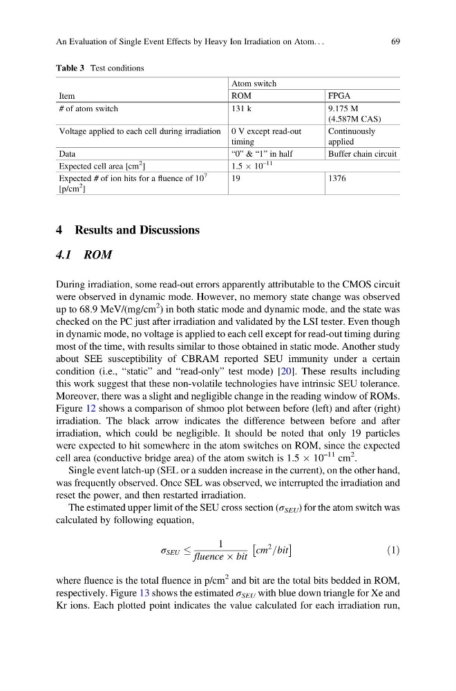
irradiation, which could be negligible. It should be noted that only 19 particles
were expected to hit somewhere in the atom switches on ROM, since the expected
cell area (conductive bridge area) of the atom switch is 1.5 Â 10
–11 cm
2 .
Single event latch-up (SEL or a sudden increase in the current), on the other hand,
was frequently observed. Once SEL was observed, we interrupted the irradiation and
reset the power, and then restarted irradiation.
The estimated upper limit of the SEU cross section (σ SEU ) for the atom switch was
calculated by following equation,
σ SEU
1
fluence  bit
cm
2
=bit
Â
Ã
ð1Þ
where fluence is the total fluence in p/cm
2 and bit are the total bits bedded in ROM,
respectively. Figure 13 shows the estimated σ SEU with blue down triangle for Xe and
Kr ions. Each plotted point indicates the value calculated for each irradiation run,
Table 3 Test conditions
Item
Atom switch
ROM
FPGA
# of atom switch
131 k
9.175 M
(4.587M CAS)
Voltage applied to each cell during irradiation 0 V except read-out
timing
Continuously
applied
Data
“0” & “1” in half
Buffer chain circuit
Expected cell area [cm
2
]
1.5 Â 10
–11
Expected # of ion hits for a fluence of 10
7
[p/cm
2
]
19
1376
An Evaluation of Single Event Effects by Heavy Ion Irradiation on Atom. . .
69
4.1 ROM
During irradiation, some read-out errors apparently attributable to the CMOS circuit
were observed in dynamic mode. However, no memory state change was observed
up to 68.9 MeV/(mg/cm
2 ) in both static mode and dynamic mode, and the state was
checked on the PC just after irradiation and validated by the LSI tester. Even though
in dynamic mode, no voltage is applied to each cell except for read-out timing during
most of the time, with results similar to those obtained in static mode. Another study
about SEE susceptibility of CBRAM reported SEU immunity under a certain
condition (i.e., “static” and “read-only” test mode) [20]. These results including
this work suggest that these non-volatile technologies have intrinsic SEU tolerance.
Moreover, there was a slight and negligible change in the reading window of ROMs.
Figure 12 shows a comparison of shmoo plot between before (left) and after (right)
irradiation. The black arrow indicates the difference between before and after
irradiation, which could be negligible. It should be noted that only 19 particles
were expected to hit somewhere in the atom switches on ROM, since the expected
cell area (conductive bridge area) of the atom switch is 1.5 Â 10
–11 cm
2 .
Single event latch-up (SEL or a sudden increase in the current), on the other hand,
was frequently observed. Once SEL was observed, we interrupted the irradiation and
reset the power, and then restarted irradiation.
The estimated upper limit of the SEU cross section (σ SEU ) for the atom switch was
calculated by following equation,
σ SEU
1
fluence  bit
cm
2
=bit
Â
Ã
ð1Þ
where fluence is the total fluence in p/cm
2 and bit are the total bits bedded in ROM,
respectively. Figure 13 shows the estimated σ SEU with blue down triangle for Xe and
Kr ions. Each plotted point indicates the value calculated for each irradiation run,
Table 3 Test conditions
Item
Atom switch
ROM
FPGA
# of atom switch
131 k
9.175 M
(4.587M CAS)
Voltage applied to each cell during irradiation 0 V except read-out
timing
Continuously
applied
Data
“0” & “1” in half
Buffer chain circuit
Expected cell area [cm
2
]
1.5 Â 10
–11
Expected # of ion hits for a fluence of 10
7
[p/cm
2
]
19
1376
An Evaluation of Single Event Effects by Heavy Ion Irradiation on Atom. . .
69