

M
O
R
h
c
t
i
w
s
m
o
t
A
SRAM
32bit CPU
64x64
Programable Cell Array
2Mb-SRAM
Programming
decoders and drivers
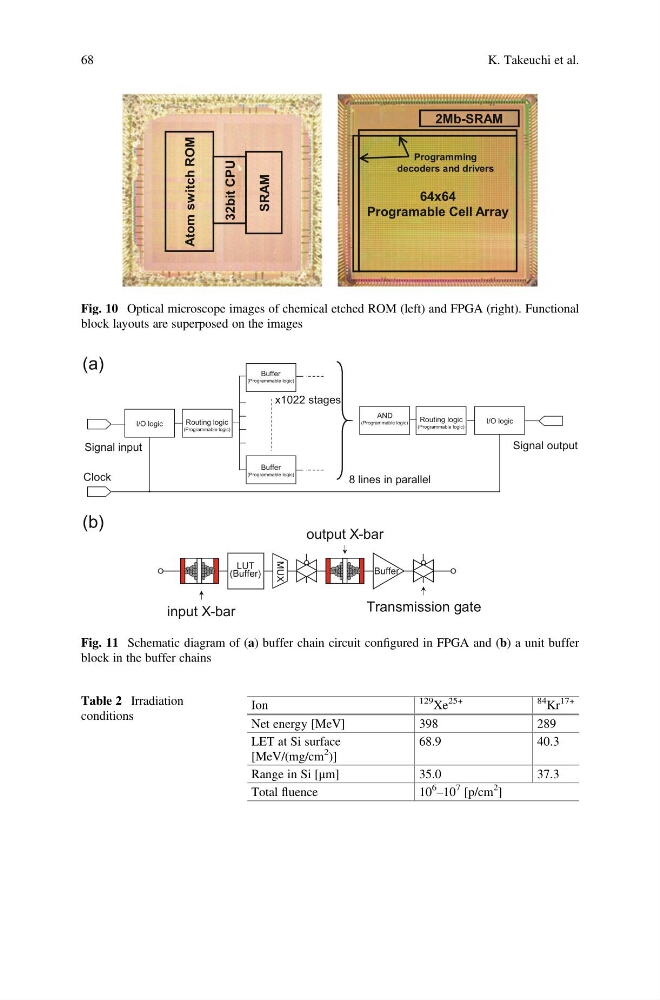
Fig. 10 Optical microscope images of chemical etched ROM (left) and FPGA (right). Functional
block layouts are superposed on the images
(a)
(b)
Signal input
Clock
I/O logic
Routing logic
(Programmable logic)
Buffer
(Programmable logic)
Buffer
(Programmable logic)
8 lines in parallel
AND
(Programmable logic)
I/O logic
Routing logic
(Programmable logic)
x1022 stages
Signal output
LUT
(Buffer)
MUX
Buffer
input X-bar
output X-bar
Transmission gate
Fig. 11 Schematic diagram of (a) buffer chain circuit configured in FPGA and (b) a unit buffer
block in the buffer chains
Table 2 Irradiation
conditions
Ion
129
Xe
25+
84
Kr
17+
Net energy [MeV]
398
289
LET at Si surface
[MeV/(mg/cm
2
)]
68.9
40.3
Range in Si [μm]
35.0
37.3
Total fluence
10
6
–10
7 [p/cm
2
]
68
K. Takeuchi et al.
O
R
h
c
t
i
w
s
m
o
t
A
SRAM
32bit CPU
64x64
Programable Cell Array
2Mb-SRAM
Programming
decoders and drivers
Fig. 10 Optical microscope images of chemical etched ROM (left) and FPGA (right). Functional
block layouts are superposed on the images
(a)
(b)
Signal input
Clock
I/O logic
Routing logic
(Programmable logic)
Buffer
(Programmable logic)
Buffer
(Programmable logic)
8 lines in parallel
AND
(Programmable logic)
I/O logic
Routing logic
(Programmable logic)
x1022 stages
Signal output
LUT
(Buffer)
MUX
Buffer
input X-bar
output X-bar
Transmission gate
Fig. 11 Schematic diagram of (a) buffer chain circuit configured in FPGA and (b) a unit buffer
block in the buffer chains
Table 2 Irradiation
conditions
Ion
129
Xe
25+
84
Kr
17+
Net energy [MeV]
398
289
LET at Si surface
[MeV/(mg/cm
2
)]
68.9
40.3
Range in Si [μm]
35.0
37.3
Total fluence
10
6
–10
7 [p/cm
2
]
68
K. Takeuchi et al.