

programmable logic tile, 100 CASs for the LUTs and 1020 CASs for the crossbar
matrix are embedded. Thus, the FPGA chip contains about nine million atom switches.
3 Experimental Setup
Both ROM and the FPGA were evaluated for radiation tolerance by using the
Takasaki Ion Accelerators for Advanced Radiation Application (TIARA) at the
National Institutes for Quantum and Radiological Science and Technology (QST).
A cocktail heavy ion beam with energy of 3.52–3.83 MeV/amu was used for the
evaluation.
The atom switches in the ROM and the FPGA were programmed for either the
ON or OFF state and validated before and after the irradiation by using the LSI tester.
Each ROM and FPGA was de-capped by chemical processes to expose the chip
surface directly to the incident ions, and mounted on a custom-made test board with
an IC socket. Figure 10 shows the chip images of the ROM (left) and the FPGA
(right). The test board was placed into a vacuum chamber at the radiation facility.
Control signal and power cables were connected via feed through terminals. The
power supply voltage and current were recorded by the HP 6629A Precision System
Power Supply located outside the vacuum chamber. “0xA” was written to ROM
(i.e., states “0” and “1” evenly written to ROM). ROM was controlled by a lap-top
PC via signal cables, and read back at one-second intervals during an irradiation run
(dynamic mode) or read back just after irradiation (static mode). The FPGA was
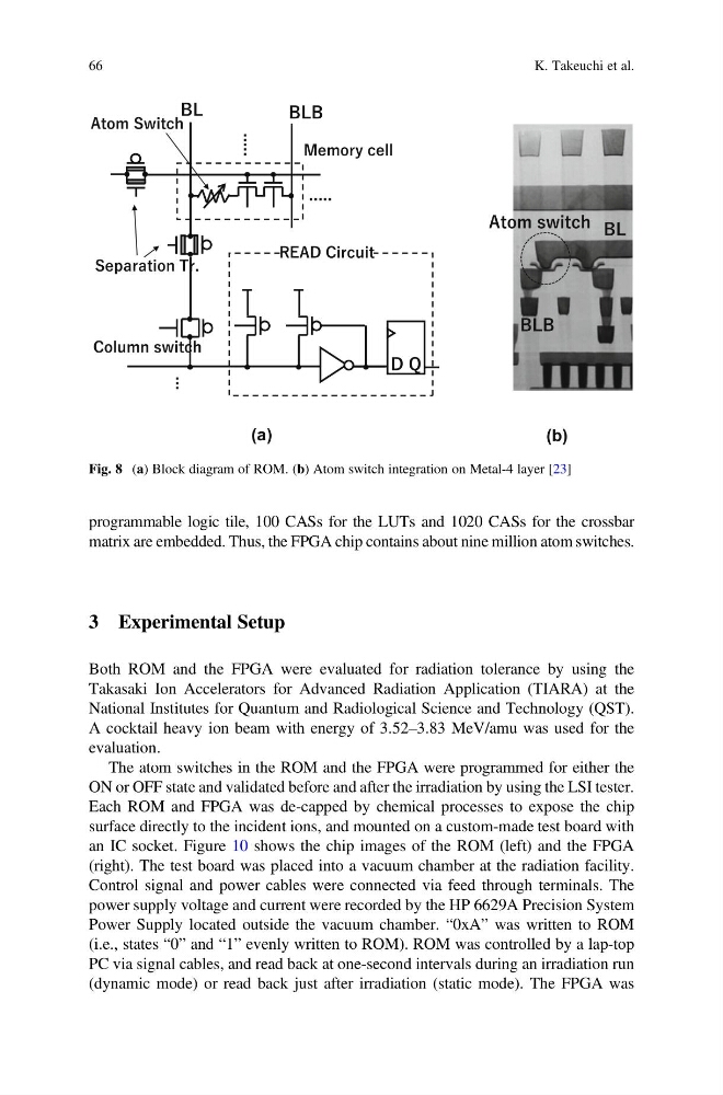
Fig. 8 (a) Block diagram of ROM. (b) Atom switch integration on Metal-4 layer [23]
66
K. Takeuchi et al.
matrix are embedded. Thus, the FPGA chip contains about nine million atom switches.
3 Experimental Setup
Both ROM and the FPGA were evaluated for radiation tolerance by using the
Takasaki Ion Accelerators for Advanced Radiation Application (TIARA) at the
National Institutes for Quantum and Radiological Science and Technology (QST).
A cocktail heavy ion beam with energy of 3.52–3.83 MeV/amu was used for the
evaluation.
The atom switches in the ROM and the FPGA were programmed for either the
ON or OFF state and validated before and after the irradiation by using the LSI tester.
Each ROM and FPGA was de-capped by chemical processes to expose the chip
surface directly to the incident ions, and mounted on a custom-made test board with
an IC socket. Figure 10 shows the chip images of the ROM (left) and the FPGA
(right). The test board was placed into a vacuum chamber at the radiation facility.
Control signal and power cables were connected via feed through terminals. The
power supply voltage and current were recorded by the HP 6629A Precision System
Power Supply located outside the vacuum chamber. “0xA” was written to ROM
(i.e., states “0” and “1” evenly written to ROM). ROM was controlled by a lap-top
PC via signal cables, and read back at one-second intervals during an irradiation run
(dynamic mode) or read back just after irradiation (static mode). The FPGA was
Fig. 8 (a) Block diagram of ROM. (b) Atom switch integration on Metal-4 layer [23]
66
K. Takeuchi et al.