

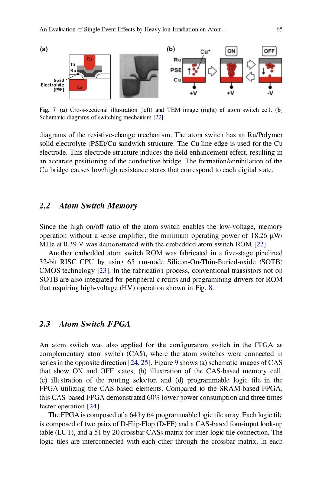
diagrams of the resistive-change mechanism. The atom switch has an Ru/Polymer
solid electrolyte (PSE)/Cu sandwich structure. The Cu line edge is used for the Cu
electrode. This electrode structure induces the field enhancement effect, resulting in
an accurate positioning of the conductive bridge. The formation/annihilation of the
Cu bridge causes low/high resistance states that correspond to each digital state.
2.2 Atom Switch Memory
Since the high on/off ratio of the atom switch enables the low-voltage, memory
operation without a sense amplifier, the minimum operating power of 18.26 μW/
MHz at 0.39 V was demonstrated with the embedded atom switch ROM [22].
Another embedded atom switch ROM was fabricated in a five-stage pipelined
32-bit RISC CPU by using 65 nm-node Silicon-On-Thin-Buried-oxide (SOTB)
CMOS technology [23]. In the fabrication process, conventional transistors not on
SOTB are also integrated for peripheral circuits and programming drivers for ROM
that requiring high-voltage (HV) operation shown in Fig. 8.
2.3 Atom Switch FPGA
An atom switch was also applied for the configuration switch in the FPGA as
complementary atom switch (CAS), where the atom switches were connected in
series in the opposite direction [24, 25]. Figure 9 shows (a) schematic images of CAS
that show ON and OFF states, (b) illustration of the CAS-based memory cell,
(c) illustration of the routing selector, and (d) programmable logic tile in the
FPGA utilizing the CAS-based elements. Compared to the SRAM-based FPGA,
this CAS-based FPGA demonstrated 60% lower power consumption and three times
faster operation [24].
The FPGA is composed of a 64 by 64 programmable logic tile array. Each logic tile
is composed of two pairs of D-Flip-Flop (D-FF) and a CAS-based four-input look-up
table (LUT), and a 51 by 20 crossbar CASs matrix for inter-logic tile connection. The
logic tiles are interconnected with each other through the crossbar matrix. In each
(a)
(b)
Ru
Solid
Electrolyte
(PSE)
Cu
Ta
Cu
Fig. 7 (a) Cross-sectional illustration (left) and TEM image (right) of atom switch cell. (b)
Schematic diagrams of switching mechanism [22]
An Evaluation of Single Event Effects by Heavy Ion Irradiation on Atom. . .
65
solid electrolyte (PSE)/Cu sandwich structure. The Cu line edge is used for the Cu
electrode. This electrode structure induces the field enhancement effect, resulting in
an accurate positioning of the conductive bridge. The formation/annihilation of the
Cu bridge causes low/high resistance states that correspond to each digital state.
2.2 Atom Switch Memory
Since the high on/off ratio of the atom switch enables the low-voltage, memory
operation without a sense amplifier, the minimum operating power of 18.26 μW/
MHz at 0.39 V was demonstrated with the embedded atom switch ROM [22].
Another embedded atom switch ROM was fabricated in a five-stage pipelined
32-bit RISC CPU by using 65 nm-node Silicon-On-Thin-Buried-oxide (SOTB)
CMOS technology [23]. In the fabrication process, conventional transistors not on
SOTB are also integrated for peripheral circuits and programming drivers for ROM
that requiring high-voltage (HV) operation shown in Fig. 8.
2.3 Atom Switch FPGA
An atom switch was also applied for the configuration switch in the FPGA as
complementary atom switch (CAS), where the atom switches were connected in
series in the opposite direction [24, 25]. Figure 9 shows (a) schematic images of CAS
that show ON and OFF states, (b) illustration of the CAS-based memory cell,
(c) illustration of the routing selector, and (d) programmable logic tile in the
FPGA utilizing the CAS-based elements. Compared to the SRAM-based FPGA,
this CAS-based FPGA demonstrated 60% lower power consumption and three times
faster operation [24].
The FPGA is composed of a 64 by 64 programmable logic tile array. Each logic tile
is composed of two pairs of D-Flip-Flop (D-FF) and a CAS-based four-input look-up
table (LUT), and a 51 by 20 crossbar CASs matrix for inter-logic tile connection. The
logic tiles are interconnected with each other through the crossbar matrix. In each
(a)
(b)
Ru
Solid
Electrolyte
(PSE)
Cu
Ta
Cu
Fig. 7 (a) Cross-sectional illustration (left) and TEM image (right) of atom switch cell. (b)
Schematic diagrams of switching mechanism [22]
An Evaluation of Single Event Effects by Heavy Ion Irradiation on Atom. . .
65