

whole processor functions are implemented in one chip, and interface circuits over
devices are eliminated. This miniaturization was realized by the high level behavioral synthesis tool CyberWorkBench (CWB). The functions of whole signal processor were written in C language. Once an optimized ALU is implemented, the
ALU was used in a series of operation process several times, and an optimized circuit
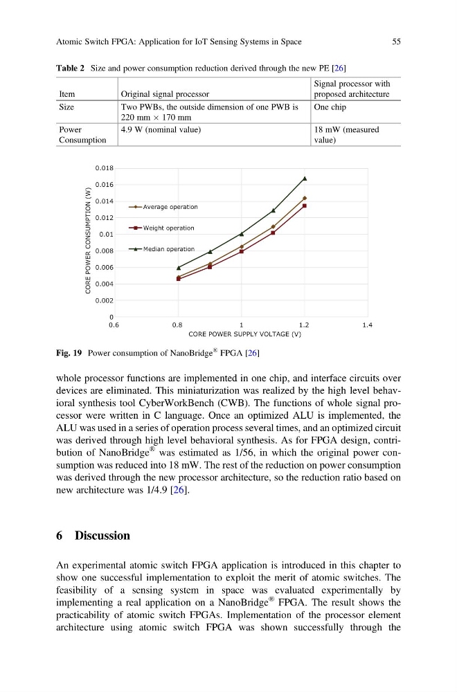
was derived through high level behavioral synthesis. As for FPGA design, contribution of NanoBridge
® was estimated as 1/56, in which the original power consumption was reduced into 18 mW. The rest of the reduction on power consumption
was derived through the new processor architecture, so the reduction ratio based on
new architecture was 1/4.9 [26].
6 Discussion
An experimental atomic switch FPGA application is introduced in this chapter to
show one successful implementation to exploit the merit of atomic switches. The
feasibility of a sensing system in space was evaluated experimentally by
implementing a real application on a NanoBridge
® FPGA. The result shows the
practicability of atomic switch FPGAs. Implementation of the processor element
architecture using atomic switch FPGA was shown successfully through the
Table 2 Size and power consumption reduction derived through the new PE [26]
Item
Original signal processor
Signal processor with
proposed architecture
Size
Two PWBs, the outside dimension of one PWB is
220 mm  170 mm
One chip
Power
Consumption
4.9 W (nominal value)
18 mW (measured
value)
0
0.002
0.004
0.006
0.008
0.01
0.012
0.014
0.016
0.018
0.6
0.8
1
1.2
1.4
CORE POWER CONSUMPTION (W)
CORE POWER SUPPLY VOLTAGE (V)
Average operation
Weight operation
Median operation
Fig. 19 Power consumption of NanoBridge
® FPGA [26]
Atomic Switch FPGA: Application for IoT Sensing Systems in Space
55
devices are eliminated. This miniaturization was realized by the high level behavioral synthesis tool CyberWorkBench (CWB). The functions of whole signal processor were written in C language. Once an optimized ALU is implemented, the
ALU was used in a series of operation process several times, and an optimized circuit
was derived through high level behavioral synthesis. As for FPGA design, contribution of NanoBridge
® was estimated as 1/56, in which the original power consumption was reduced into 18 mW. The rest of the reduction on power consumption
was derived through the new processor architecture, so the reduction ratio based on
new architecture was 1/4.9 [26].
6 Discussion
An experimental atomic switch FPGA application is introduced in this chapter to
show one successful implementation to exploit the merit of atomic switches. The
feasibility of a sensing system in space was evaluated experimentally by
implementing a real application on a NanoBridge
® FPGA. The result shows the
practicability of atomic switch FPGAs. Implementation of the processor element
architecture using atomic switch FPGA was shown successfully through the
Table 2 Size and power consumption reduction derived through the new PE [26]
Item
Original signal processor
Signal processor with
proposed architecture
Size
Two PWBs, the outside dimension of one PWB is
220 mm  170 mm
One chip
Power
Consumption
4.9 W (nominal value)
18 mW (measured
value)
0
0.002
0.004
0.006
0.008
0.01
0.012
0.014
0.016
0.018
0.6
0.8
1
1.2
1.4
CORE POWER CONSUMPTION (W)
CORE POWER SUPPLY VOLTAGE (V)
Average operation
Weight operation
Median operation
Fig. 19 Power consumption of NanoBridge
® FPGA [26]
Atomic Switch FPGA: Application for IoT Sensing Systems in Space
55