

500 mW, which was estimated from the power consumption of the whole electronics
unit and design schematics.
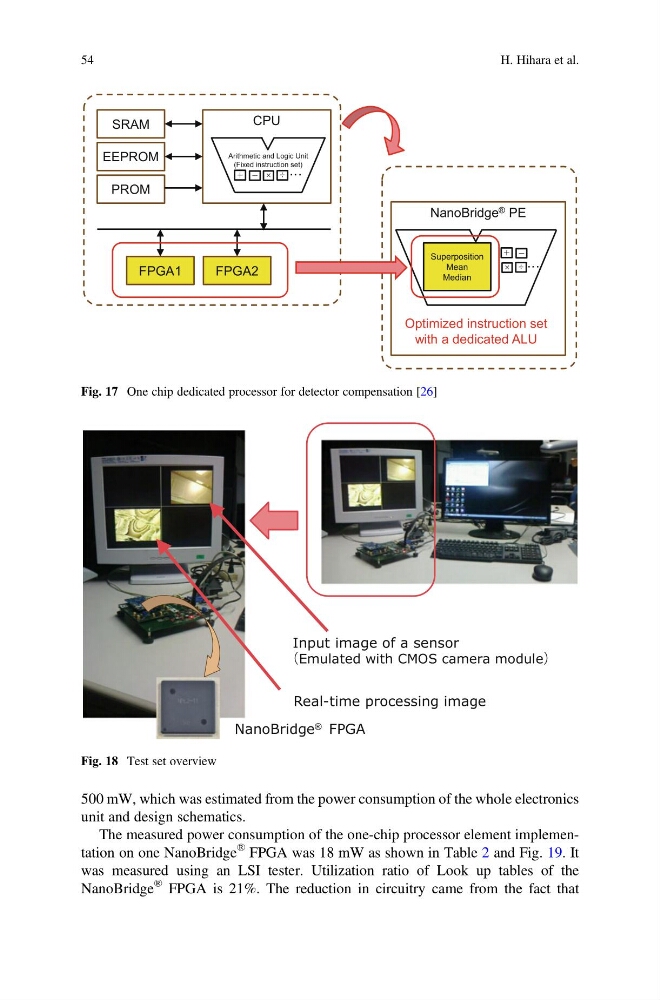
The measured power consumption of the one-chip processor element implementation on one NanoBridge
® FPGA was 18 mW as shown in Table 2 and Fig. 19. It
was measured using an LSI tester. Utilization ratio of Look up tables of the
NanoBridge
® FPGA is 21%. The reduction in circuitry came from the fact that
CPU
SRAM
EEPROM
PROM
¼ Ù
Arithmetic and Logic Unit
(Fixed instruction set)
FPGA1
FPGA2
NanoBridge ® PE
¼ Ù
Optimized instruction set
with a dedicated ALU
Superposition
Mean
Median
Fig. 17 One chip dedicated processor for detector compensation [26]
Input image of a sensor
Emulated with CMOS camera module
Real-time processing image
NanoBridge ® FPGA
Fig. 18 Test set overview
54
H. Hihara et al.
unit and design schematics.
The measured power consumption of the one-chip processor element implementation on one NanoBridge
® FPGA was 18 mW as shown in Table 2 and Fig. 19. It
was measured using an LSI tester. Utilization ratio of Look up tables of the
NanoBridge
® FPGA is 21%. The reduction in circuitry came from the fact that
CPU
SRAM
EEPROM
PROM
¼ Ù
Arithmetic and Logic Unit
(Fixed instruction set)
FPGA1
FPGA2
NanoBridge ® PE
¼ Ù
Optimized instruction set
with a dedicated ALU
Superposition
Mean
Median
Fig. 17 One chip dedicated processor for detector compensation [26]
Input image of a sensor
Emulated with CMOS camera module
Real-time processing image
NanoBridge ® FPGA
Fig. 18 Test set overview
54
H. Hihara et al.