

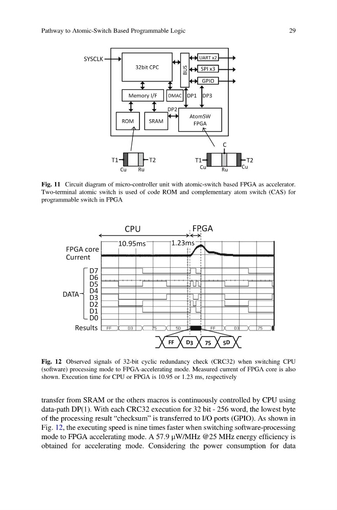
transfer from SRAM or the others macros is continuously controlled by CPU using
data-path DP(1). With each CRC32 execution for 32 bit - 256 word, the lowest byte
of the processing result “checksum” is transferred to I/O ports (GPIO). As shown in
Fig. 12, the executing speed is nine times faster when switching software-processing
mode to FPGA accelerating mode. A 57.9 μW/MHz @25 MHz energy efficiency is
obtained for accelerating mode. Considering the power consumption for data
UART x2
SPI x3
GPIO
BUS
SRAM
Memory I/F
32bit CPC
ROM
AtomSW
FPGA
DMAC
SYSCLK
DP1 DP3
DP2
Cu
T1
T2
C
Cu
Ru
Cu
T1
T2
Ru
Fig. 11 Circuit diagram of micro-controller unit with atomic-switch based FPGA as accelerator.
Two-terminal atomic switch is used of code ROM and complementary atom switch (CAS) for
programmable switch in FPGA
10.95ms
1.23ms
CPU
FPGA
DATA
FPGA core
Current
FF
D3
75
5D
Results
D0
D7
D6
D5
D4
D3
D2
D1
Fig. 12 Observed signals of 32-bit cyclic redundancy check (CRC32) when switching CPU
(software) processing mode to FPGA-accelerating mode. Measured current of FPGA core is also
shown. Execution time for CPU or FPGA is 10.95 or 1.23 ms, respectively
Pathway to Atomic-Switch Based Programmable Logic
29
data-path DP(1). With each CRC32 execution for 32 bit - 256 word, the lowest byte
of the processing result “checksum” is transferred to I/O ports (GPIO). As shown in
Fig. 12, the executing speed is nine times faster when switching software-processing
mode to FPGA accelerating mode. A 57.9 μW/MHz @25 MHz energy efficiency is
obtained for accelerating mode. Considering the power consumption for data
UART x2
SPI x3
GPIO
BUS
SRAM
Memory I/F
32bit CPC
ROM
AtomSW
FPGA
DMAC
SYSCLK
DP1 DP3
DP2
Cu
T1
T2
C
Cu
Ru
Cu
T1
T2
Ru
Fig. 11 Circuit diagram of micro-controller unit with atomic-switch based FPGA as accelerator.
Two-terminal atomic switch is used of code ROM and complementary atom switch (CAS) for
programmable switch in FPGA
10.95ms
1.23ms
CPU
FPGA
DATA
FPGA core
Current
FF
D3
75
5D
Results
D0
D7
D6
D5
D4
D3
D2
D1
Fig. 12 Observed signals of 32-bit cyclic redundancy check (CRC32) when switching CPU
(software) processing mode to FPGA-accelerating mode. Measured current of FPGA core is also
shown. Execution time for CPU or FPGA is 10.95 or 1.23 ms, respectively
Pathway to Atomic-Switch Based Programmable Logic
29