

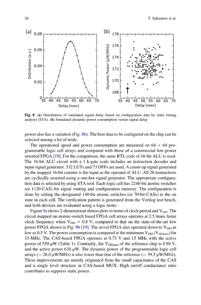
power also has a variation (Fig. 8b). The best data to be configured on the chip can be
selected among a lot of trials.
The operational speed and power consumption are measured on 64 Â 64 programmable logic cell arrays and compared with those of a commercial low-power
oriented FPGA [19]. For the comparison, the same RTL code of 16-bit ALU is used.
The 16-bit ALU circuit with a 1 k-gate scale includes an instruction decoder and
input signal generator. 332 LUTs and 73 DFFs are used. A count-up signal generated
by the mapped 16-bit counter is the input as the operand of ALU. All 28 instructions
are cyclically asserted using a one-hot signal generator. The appropriate configuration data is selected by using STA tool. Each logic cell has 2240-bit atomic switches
(or 1120 CAS) for signal routing and configuration memory. The configuration is
done by setting the designated 140-bit atomic switches (or 70-bit CASs) to the on
state in each cell. The verification pattern is generated from the Verilog test bench,
and both devices are evaluated using a logic tester.
Figure 9a shows 2-dimensional shmoo plots in terms of clock period and V DD . The
circuit mapped on atomic-switch based FPGA cell arrays operates at 2.5 times faster
clock frequency when V DD ¼ 0.8 V, compared to that on the state-of-the-art low
power FPGA shown in Fig. 9b [19]. The novel FPGA also operated down to V DD as
low as 0.5 V. The power consumption is compared at the minimum V DD (V DDmin ) for
15-MHz. The CAS-based FPGA operates at 0.73 V and 15 MHz with the active
power of 550 μW (Table 1). Contrarily, the V DDmin of the reference chip is 0.94 V,
and the active power 630 μW. The dynamic power of the programmable logic cell
arrays (¼ 28.0 μW/MHz) is also lower than that of the reference (¼ 39.5 μW/MHz).
These improvements are mainly originated from the small capacitance of the CAS
and a single level structure in CAS-based MUX. High on/off conductance ratio
contributes to suppress static power.
Dynamic Power (µW/MHz)
Delay (nsec)
Delay (nsec)
Distribution (a.u.)
(a)
(b)
Fig. 8 (a) Distribution of simulated signal delay based on configuration data by static timing
analysis (STA). (b) Simulated dynamic power consumption versus signal delay
26
T. Sakamoto et al.
selected among a lot of trials.
The operational speed and power consumption are measured on 64 Â 64 programmable logic cell arrays and compared with those of a commercial low-power
oriented FPGA [19]. For the comparison, the same RTL code of 16-bit ALU is used.
The 16-bit ALU circuit with a 1 k-gate scale includes an instruction decoder and
input signal generator. 332 LUTs and 73 DFFs are used. A count-up signal generated
by the mapped 16-bit counter is the input as the operand of ALU. All 28 instructions
are cyclically asserted using a one-hot signal generator. The appropriate configuration data is selected by using STA tool. Each logic cell has 2240-bit atomic switches
(or 1120 CAS) for signal routing and configuration memory. The configuration is
done by setting the designated 140-bit atomic switches (or 70-bit CASs) to the on
state in each cell. The verification pattern is generated from the Verilog test bench,
and both devices are evaluated using a logic tester.
Figure 9a shows 2-dimensional shmoo plots in terms of clock period and V DD . The
circuit mapped on atomic-switch based FPGA cell arrays operates at 2.5 times faster
clock frequency when V DD ¼ 0.8 V, compared to that on the state-of-the-art low
power FPGA shown in Fig. 9b [19]. The novel FPGA also operated down to V DD as
low as 0.5 V. The power consumption is compared at the minimum V DD (V DDmin ) for
15-MHz. The CAS-based FPGA operates at 0.73 V and 15 MHz with the active
power of 550 μW (Table 1). Contrarily, the V DDmin of the reference chip is 0.94 V,
and the active power 630 μW. The dynamic power of the programmable logic cell
arrays (¼ 28.0 μW/MHz) is also lower than that of the reference (¼ 39.5 μW/MHz).
These improvements are mainly originated from the small capacitance of the CAS
and a single level structure in CAS-based MUX. High on/off conductance ratio
contributes to suppress static power.
Dynamic Power (µW/MHz)
Delay (nsec)
Delay (nsec)
Distribution (a.u.)
(a)
(b)
Fig. 8 (a) Distribution of simulated signal delay based on configuration data by static timing
analysis (STA). (b) Simulated dynamic power consumption versus signal delay
26
T. Sakamoto et al.