

the electrolyte, thereby resulting in forming-less programming, which is required to
ReRAM with metal oxide resistive layer.
Logic function is demonstrated by mapping the application on the fabricated
programmable logic. The configuration data for CAS is generated by in-house
design-automation tools. The tool chain is composed of LUT-mapping,
CLB-clustering, and placement and routing (P&R) tools. The tool chain generates
the configuration data from a resistor-transfer-level (RTL) code. First, the gate level
netlist is prepared by logic synthesis. Then, the gate level netlist are converted into the
format comprising of 4-input LUT and DFF. Up to 2 pairs of LUT and DFF are
configurable corresponding to the CLB. Then, a P&R is carried out and the binary
data to program CAS is generated. The developed static timing analysis (STA) tool
evaluates a signal delay. The difference from the existing STA tool for SRAM-based
FPGA is that the tool is necessary to prepare a variety of primitives in accordance with
the on/off state of CAS in these primitives. The propagation delay primarily depends
on the number of the on-state CAS, because the capacitive load of output line of
crossbar is coupled by the on-state CAS. The dynamic power consumption is also
calculated by the power analyzer tool, so as to optimize the configuration data before
programming. Figure 8 shows the results of STA and power analyzer on the configuration data generated by the tool chain. A 16-bit arithmetic logic unit (ALU) circuit
is used for application circuit. The obtained signal delay in a critical path has various
values for each configuration data, ranging from 40 to 65 ns. The variation is
originated from the nature of simulated annealing used in the tool chain. The dynamic
100nm
Y
X
C
M7
M6
M5
M4
M3
M2
M1
64x64
Logic Cell
Array
(a)
(c)
(b)
(d)
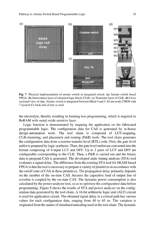
Fig. 7 Physical implementation of atomic switch in integrated circuit. (a) Atomic-switch based
FPGA. (b) Interconnect layer of clustered logic block (CLB). (c) Transistor layer of CLB. (d) Cross
sectional view of chip. Atomic switch is integrated between Metal 4 and 5. 65 nm-node CMOS with
7 layered Cu back-end of line is used
Pathway to Atomic-Switch Based Programmable Logic
25
ReRAM with metal oxide resistive layer.
Logic function is demonstrated by mapping the application on the fabricated
programmable logic. The configuration data for CAS is generated by in-house
design-automation tools. The tool chain is composed of LUT-mapping,
CLB-clustering, and placement and routing (P&R) tools. The tool chain generates
the configuration data from a resistor-transfer-level (RTL) code. First, the gate level
netlist is prepared by logic synthesis. Then, the gate level netlist are converted into the
format comprising of 4-input LUT and DFF. Up to 2 pairs of LUT and DFF are
configurable corresponding to the CLB. Then, a P&R is carried out and the binary
data to program CAS is generated. The developed static timing analysis (STA) tool
evaluates a signal delay. The difference from the existing STA tool for SRAM-based
FPGA is that the tool is necessary to prepare a variety of primitives in accordance with
the on/off state of CAS in these primitives. The propagation delay primarily depends
on the number of the on-state CAS, because the capacitive load of output line of
crossbar is coupled by the on-state CAS. The dynamic power consumption is also
calculated by the power analyzer tool, so as to optimize the configuration data before
programming. Figure 8 shows the results of STA and power analyzer on the configuration data generated by the tool chain. A 16-bit arithmetic logic unit (ALU) circuit
is used for application circuit. The obtained signal delay in a critical path has various
values for each configuration data, ranging from 40 to 65 ns. The variation is
originated from the nature of simulated annealing used in the tool chain. The dynamic
100nm
Y
X
C
M7
M6
M5
M4
M3
M2
M1
64x64
Logic Cell
Array
(a)
(c)
(b)
(d)
Fig. 7 Physical implementation of atomic switch in integrated circuit. (a) Atomic-switch based
FPGA. (b) Interconnect layer of clustered logic block (CLB). (c) Transistor layer of CLB. (d) Cross
sectional view of chip. Atomic switch is integrated between Metal 4 and 5. 65 nm-node CMOS with
7 layered Cu back-end of line is used
Pathway to Atomic-Switch Based Programmable Logic
25