

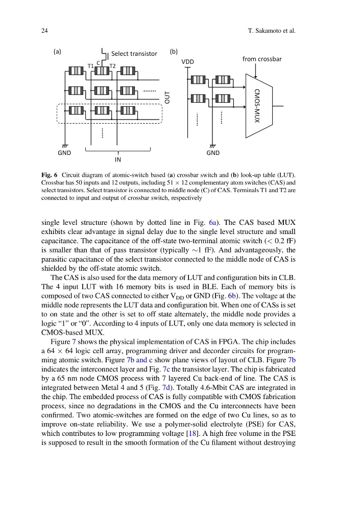
single level structure (shown by dotted line in Fig. 6a). The CAS based MUX
exhibits clear advantage in signal delay due to the single level structure and small
capacitance. The capacitance of the off-state two-terminal atomic switch (< 0.2 fF)
is smaller than that of pass transistor (typically $1 fF). And advantageously, the
parasitic capacitance of the select transistor connected to the middle node of CAS is
shielded by the off-state atomic switch.
The CAS is also used for the data memory of LUT and configuration bits in CLB.
The 4 input LUT with 16 memory bits is used in BLE. Each of memory bits is
composed of two CAS connected to either V DD or GND (Fig. 6b). The voltage at the
middle node represents the LUT data and configuration bit. When one of CASs is set
to on state and the other is set to off state alternately, the middle node provides a
logic “1” or “0”. According to 4 inputs of LUT, only one data memory is selected in
CMOS-based MUX.
Figure 7 shows the physical implementation of CAS in FPGA. The chip includes
a 64 Â 64 logic cell array, programming driver and decorder circuits for programming atomic switch. Figure 7b and c show plane views of layout of CLB. Figure 7b
indicates the interconnect layer and Fig. 7c the transistor layer. The chip is fabricated
by a 65 nm node CMOS process with 7 layered Cu back-end of line. The CAS is
integrated between Metal 4 and 5 (Fig. 7d). Totally 4.6-Mbit CAS are integrated in
the chip. The embedded process of CAS is fully compatible with CMOS fabrication
process, since no degradations in the CMOS and the Cu interconnects have been
confirmed. Two atomic-switches are formed on the edge of two Cu lines, so as to
improve on-state reliability. We use a polymer-solid electrolyte (PSE) for CAS,
which contributes to low programming voltage [18]. A high free volume in the PSE
is supposed to result in the smooth formation of the Cu filament without destroying
from crossbar
CMOS-MUX
VDD
GND
IN
OUT
(a)
(b)
Select transistor
T1
T2
C
GND
Fig. 6 Circuit diagram of atomic-switch based (a) crossbar switch and (b) look-up table (LUT).
Crossbar has 50 inputs and 12 outputs, including 51 Â 12 complementary atom switches (CAS) and
select transistors. Select transistor is connected to middle node (C) of CAS. Terminals T1 and T2 are
connected to input and output of crossbar switch, respectively
24
T. Sakamoto et al.
exhibits clear advantage in signal delay due to the single level structure and small
capacitance. The capacitance of the off-state two-terminal atomic switch (< 0.2 fF)
is smaller than that of pass transistor (typically $1 fF). And advantageously, the
parasitic capacitance of the select transistor connected to the middle node of CAS is
shielded by the off-state atomic switch.
The CAS is also used for the data memory of LUT and configuration bits in CLB.
The 4 input LUT with 16 memory bits is used in BLE. Each of memory bits is
composed of two CAS connected to either V DD or GND (Fig. 6b). The voltage at the
middle node represents the LUT data and configuration bit. When one of CASs is set
to on state and the other is set to off state alternately, the middle node provides a
logic “1” or “0”. According to 4 inputs of LUT, only one data memory is selected in
CMOS-based MUX.
Figure 7 shows the physical implementation of CAS in FPGA. The chip includes
a 64 Â 64 logic cell array, programming driver and decorder circuits for programming atomic switch. Figure 7b and c show plane views of layout of CLB. Figure 7b
indicates the interconnect layer and Fig. 7c the transistor layer. The chip is fabricated
by a 65 nm node CMOS process with 7 layered Cu back-end of line. The CAS is
integrated between Metal 4 and 5 (Fig. 7d). Totally 4.6-Mbit CAS are integrated in
the chip. The embedded process of CAS is fully compatible with CMOS fabrication
process, since no degradations in the CMOS and the Cu interconnects have been
confirmed. Two atomic-switches are formed on the edge of two Cu lines, so as to
improve on-state reliability. We use a polymer-solid electrolyte (PSE) for CAS,
which contributes to low programming voltage [18]. A high free volume in the PSE
is supposed to result in the smooth formation of the Cu filament without destroying
from crossbar
CMOS-MUX
VDD
GND
IN
OUT
(a)
(b)
Select transistor
T1
T2
C
GND
Fig. 6 Circuit diagram of atomic-switch based (a) crossbar switch and (b) look-up table (LUT).
Crossbar has 50 inputs and 12 outputs, including 51 Â 12 complementary atom switches (CAS) and
select transistors. Select transistor is connected to middle node (C) of CAS. Terminals T1 and T2 are
connected to input and output of crossbar switch, respectively
24
T. Sakamoto et al.