

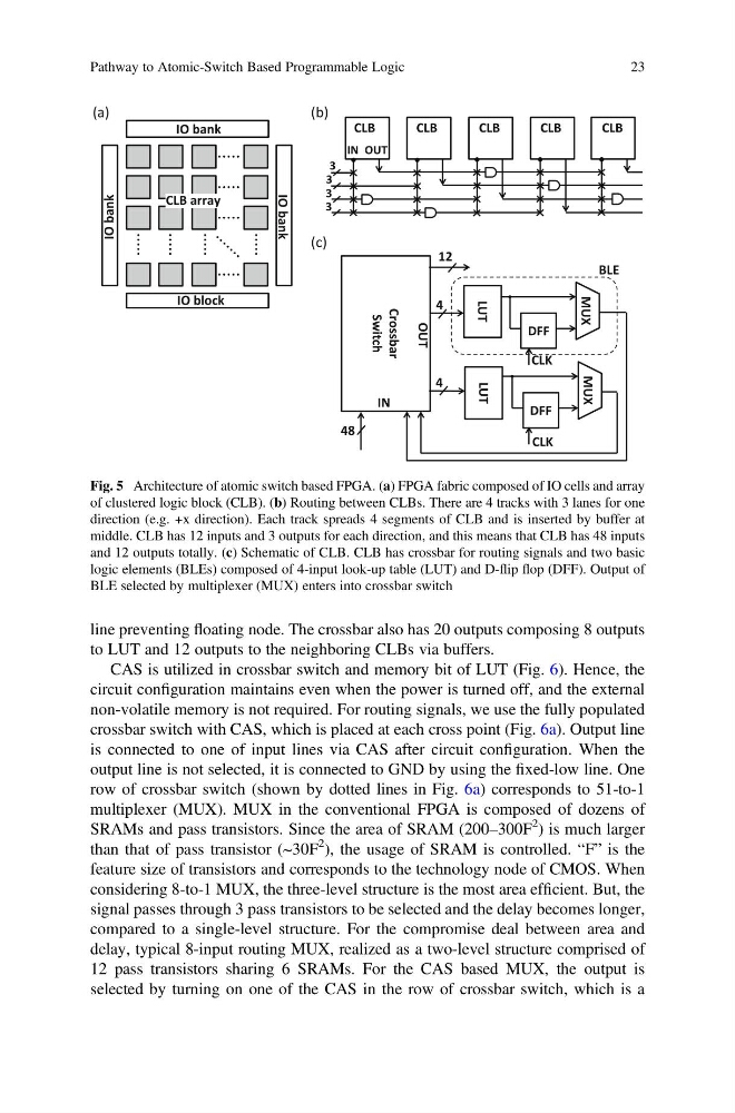
line preventing floating node. The crossbar also has 20 outputs composing 8 outputs
to LUT and 12 outputs to the neighboring CLBs via buffers.
CAS is utilized in crossbar switch and memory bit of LUT (Fig. 6). Hence, the
circuit configuration maintains even when the power is turned off, and the external
non-volatile memory is not required. For routing signals, we use the fully populated
crossbar switch with CAS, which is placed at each cross point (Fig. 6a). Output line
is connected to one of input lines via CAS after circuit configuration. When the
output line is not selected, it is connected to GND by using the fixed-low line. One
row of crossbar switch (shown by dotted lines in Fig. 6a) corresponds to 51-to-1
multiplexer (MUX). MUX in the conventional FPGA is composed of dozens of
SRAMs and pass transistors. Since the area of SRAM (200–300F
2
) is much larger
than that of pass transistor (~30F
2 ), the usage of SRAM is controlled. “F” is the
feature size of transistors and corresponds to the technology node of CMOS. When
considering 8-to-1 MUX, the three-level structure is the most area efficient. But, the
signal passes through 3 pass transistors to be selected and the delay becomes longer,
compared to a single-level structure. For the compromise deal between area and
delay, typical 8-input routing MUX, realized as a two-level structure comprised of
12 pass transistors sharing 6 SRAMs. For the CAS based MUX, the output is
selected by turning on one of the CAS in the row of crossbar switch, which is a
IO bank
k
n
a
b
O
I
IO bank
CLB array
IO block
(a)
(b)
3
3
3
3
CLB
IN OUT
CLB
CLB
CLB
CLB
(c)
Crossbar
Switch
LUT
LUT
DFF
MUX
CLK
MUX
CLK
48
DFF
4
4
12
IN
OUT
BLE
Fig. 5 Architecture of atomic switch based FPGA. (a) FPGA fabric composed of IO cells and array
of clustered logic block (CLB). (b) Routing between CLBs. There are 4 tracks with 3 lanes for one
direction (e.g. +x direction). Each track spreads 4 segments of CLB and is inserted by buffer at
middle. CLB has 12 inputs and 3 outputs for each direction, and this means that CLB has 48 inputs
and 12 outputs totally. (c) Schematic of CLB. CLB has crossbar for routing signals and two basic
logic elements (BLEs) composed of 4-input look-up table (LUT) and D-flip flop (DFF). Output of
BLE selected by multiplexer (MUX) enters into crossbar switch
Pathway to Atomic-Switch Based Programmable Logic
23
to LUT and 12 outputs to the neighboring CLBs via buffers.
CAS is utilized in crossbar switch and memory bit of LUT (Fig. 6). Hence, the
circuit configuration maintains even when the power is turned off, and the external
non-volatile memory is not required. For routing signals, we use the fully populated
crossbar switch with CAS, which is placed at each cross point (Fig. 6a). Output line
is connected to one of input lines via CAS after circuit configuration. When the
output line is not selected, it is connected to GND by using the fixed-low line. One
row of crossbar switch (shown by dotted lines in Fig. 6a) corresponds to 51-to-1
multiplexer (MUX). MUX in the conventional FPGA is composed of dozens of
SRAMs and pass transistors. Since the area of SRAM (200–300F
2
) is much larger
than that of pass transistor (~30F
2 ), the usage of SRAM is controlled. “F” is the
feature size of transistors and corresponds to the technology node of CMOS. When
considering 8-to-1 MUX, the three-level structure is the most area efficient. But, the
signal passes through 3 pass transistors to be selected and the delay becomes longer,
compared to a single-level structure. For the compromise deal between area and
delay, typical 8-input routing MUX, realized as a two-level structure comprised of
12 pass transistors sharing 6 SRAMs. For the CAS based MUX, the output is
selected by turning on one of the CAS in the row of crossbar switch, which is a
IO bank
k
n
a
b
O
I
IO bank
CLB array
IO block
(a)
(b)
3
3
3
3
CLB
IN OUT
CLB
CLB
CLB
CLB
(c)
Crossbar
Switch
LUT
LUT
DFF
MUX
CLK
MUX
CLK
48
DFF
4
4
12
IN
OUT
BLE
Fig. 5 Architecture of atomic switch based FPGA. (a) FPGA fabric composed of IO cells and array
of clustered logic block (CLB). (b) Routing between CLBs. There are 4 tracks with 3 lanes for one
direction (e.g. +x direction). Each track spreads 4 segments of CLB and is inserted by buffer at
middle. CLB has 12 inputs and 3 outputs for each direction, and this means that CLB has 48 inputs
and 12 outputs totally. (c) Schematic of CLB. CLB has crossbar for routing signals and two basic
logic elements (BLEs) composed of 4-input look-up table (LUT) and D-flip flop (DFF). Output of
BLE selected by multiplexer (MUX) enters into crossbar switch
Pathway to Atomic-Switch Based Programmable Logic
23