

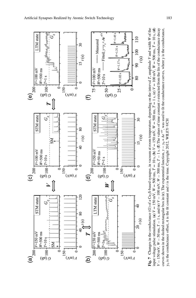
Fig. 7
Changes in the conductance (G) of a Cu
2 S-based synapse, in vacuum at room temperature, depending on the interval T,
amplitude V
and width W
of the
input voltage pulse stimulation. (a) V
¼ 150 mV, W
¼ 500 ms, T
¼ 10 s, (b) V
¼ 150 mV, W
¼ 500 ms, T
¼ 1 s, (c) V
¼ 100 mV, W
¼ 500 ms, T
¼ 10 s, (d)
V
¼ 150 mV, W
¼ 50 ms, T
¼ 1 s, and (e) V
¼ 100 mV, W
¼ 500 ms, T
¼ 1 s. (f) The values of time constant
τ extracted from the
fits of the conductance decay
curves shown in the dashed rectangular box in (c). The exponential function, y
¼ y
0 + Ae
–t/τ
, was used to
fit the conductance curves, where y is the conductance,
y
0 is the conductance offset, A
is the
fit constant and t
is the time. Copyright 2012, WILEY-VCH
Artificial Synapses Realized by Atomic Switch Technology
183
Changes in the conductance (G) of a Cu
2 S-based synapse, in vacuum at room temperature, depending on the interval T,
amplitude V
and width W
of the
input voltage pulse stimulation. (a) V
¼ 150 mV, W
¼ 500 ms, T
¼ 10 s, (b) V
¼ 150 mV, W
¼ 500 ms, T
¼ 1 s, (c) V
¼ 100 mV, W
¼ 500 ms, T
¼ 10 s, (d)
V
¼ 150 mV, W
¼ 50 ms, T
¼ 1 s, and (e) V
¼ 100 mV, W
¼ 500 ms, T
¼ 1 s. (f) The values of time constant
τ extracted from the
fits of the conductance decay
curves shown in the dashed rectangular box in (c). The exponential function, y
¼ y
0 + Ae
–t/τ
, was used to
fit the conductance curves, where y is the conductance,
y
0 is the conductance offset, A
is the
fit constant and t
is the time. Copyright 2012, WILEY-VCH
Artificial Synapses Realized by Atomic Switch Technology
183