

cluster with controlling the metal ion migration and the solid electrochemical
reaction in a mixed conductor material from the nanoscale to atomic scale level [10].
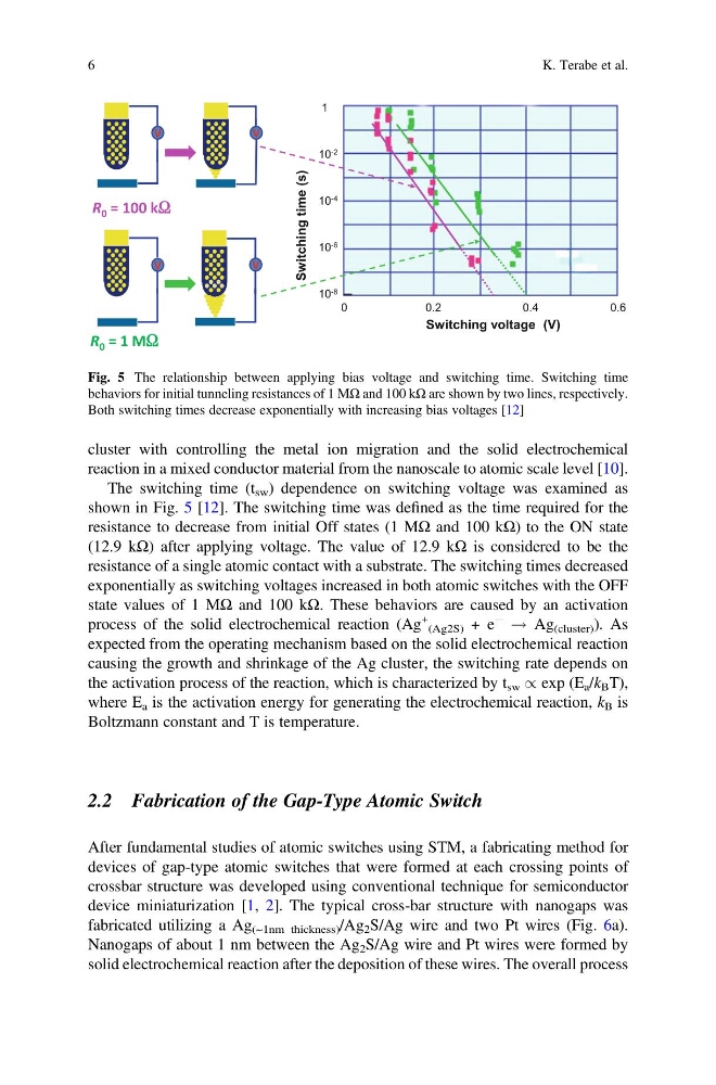
The switching time (t sw ) dependence on switching voltage was examined as
shown in Fig. 5 [12]. The switching time was defined as the time required for the
resistance to decrease from initial Off states (1 MΩ and 100 kΩ) to the ON state
(12.9 kΩ) after applying voltage. The value of 12.9 kΩ is considered to be the
resistance of a single atomic contact with a substrate. The switching times decreased
exponentially as switching voltages increased in both atomic switches with the OFF
state values of 1 MΩ and 100 kΩ. These behaviors are caused by an activation
process of the solid electrochemical reaction (Ag
+
(Ag2S) + e
À
! Ag (cluster) ). As
expected from the operating mechanism based on the solid electrochemical reaction
causing the growth and shrinkage of the Ag cluster, the switching rate depends on
the activation process of the reaction, which is characterized by t sw / exp (E a /k B T),
where E a is the activation energy for generating the electrochemical reaction, k B is
Boltzmann constant and T is temperature.
2.2 Fabrication of the Gap-Type Atomic Switch
After fundamental studies of atomic switches using STM, a fabricating method for
devices of gap-type atomic switches that were formed at each crossing points of
crossbar structure was developed using conventional technique for semiconductor
device miniaturization [1, 2]. The typical cross-bar structure with nanogaps was
fabricated utilizing a Ag (~1nm thickness) /Ag 2 S/Ag wire and two Pt wires (Fig. 6a).
Nanogaps of about 1 nm between the Ag 2 S/Ag wire and Pt wires were formed by
solid electrochemical reaction after the deposition of these wires. The overall process
Switching voltage (V)
V
V
V
V
R 0 = 100 kΩ
R 0 = 1 MΩ
Switching Ɵme (s)
Switching time (s)
1
10 -2
10 -4
10 -6
10 -8
0
0 . 2
0 . 4
0 . 6
Fig. 5 The relationship between applying bias voltage and switching time. Switching time
behaviors for initial tunneling resistances of 1 MΩ and 100 kΩ are shown by two lines, respectively.
Both switching times decrease exponentially with increasing bias voltages [12]
6
K. Terabe et al.
reaction in a mixed conductor material from the nanoscale to atomic scale level [10].
The switching time (t sw ) dependence on switching voltage was examined as
shown in Fig. 5 [12]. The switching time was defined as the time required for the
resistance to decrease from initial Off states (1 MΩ and 100 kΩ) to the ON state
(12.9 kΩ) after applying voltage. The value of 12.9 kΩ is considered to be the
resistance of a single atomic contact with a substrate. The switching times decreased
exponentially as switching voltages increased in both atomic switches with the OFF
state values of 1 MΩ and 100 kΩ. These behaviors are caused by an activation
process of the solid electrochemical reaction (Ag
+
(Ag2S) + e
À
! Ag (cluster) ). As
expected from the operating mechanism based on the solid electrochemical reaction
causing the growth and shrinkage of the Ag cluster, the switching rate depends on
the activation process of the reaction, which is characterized by t sw / exp (E a /k B T),
where E a is the activation energy for generating the electrochemical reaction, k B is
Boltzmann constant and T is temperature.
2.2 Fabrication of the Gap-Type Atomic Switch
After fundamental studies of atomic switches using STM, a fabricating method for
devices of gap-type atomic switches that were formed at each crossing points of
crossbar structure was developed using conventional technique for semiconductor
device miniaturization [1, 2]. The typical cross-bar structure with nanogaps was
fabricated utilizing a Ag (~1nm thickness) /Ag 2 S/Ag wire and two Pt wires (Fig. 6a).
Nanogaps of about 1 nm between the Ag 2 S/Ag wire and Pt wires were formed by
solid electrochemical reaction after the deposition of these wires. The overall process
Switching voltage (V)
V
V
V
V
R 0 = 100 kΩ
R 0 = 1 MΩ
Switching Ɵme (s)
Switching time (s)
1
10 -2
10 -4
10 -6
10 -8
0
0 . 2
0 . 4
0 . 6
Fig. 5 The relationship between applying bias voltage and switching time. Switching time
behaviors for initial tunneling resistances of 1 MΩ and 100 kΩ are shown by two lines, respectively.
Both switching times decrease exponentially with increasing bias voltages [12]
6
K. Terabe et al.