

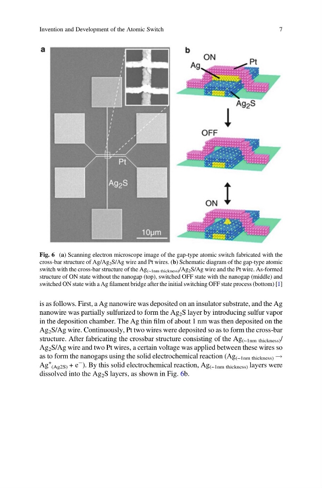
is as follows. First, a Ag nanowire was deposited on an insulator substrate, and the Ag
nanowire was partially sulfurized to form the Ag 2 S layer by introducing sulfur vapor
in the deposition chamber. The Ag thin film of about 1 nm was then deposited on the
Ag 2 S/Ag wire. Continuously, Pt two wires were deposited so as to form the cross-bar
structure. After fabricating the crossbar structure consisting of the Ag (~1nm thickness) /
Ag 2 S/Ag wire and two Pt wires, a certain voltage was applied between these wires so
as to form the nanogaps using the solid electrochemical reaction (Ag (~1nm thickness) !
Ag
+
(Ag2S) + e
À ). By this solid electrochemical reaction, Ag (~1nm thickness) layers were
dissolved into the Ag 2 S layers, as shown in Fig. 6b.
Fig. 6 (a) Scanning electron microscope image of the gap-type atomic switch fabricated with the
cross-bar structure of Ag/Ag 2 S/Ag wire and Pt wires. (b) Schematic diagram of the gap-type atomic
switch with the cross-bar structure of the Ag (~1nm thickness) /Ag 2 S/Ag wire and the Pt wire. As-formed
structure of ON state without the nanogap (top), switched OFF state with the nanogap (middle) and
switched ON state with a Ag filament bridge after the initial switching OFF state process (bottom) [1]
Invention and Development of the Atomic Switch
7
nanowire was partially sulfurized to form the Ag 2 S layer by introducing sulfur vapor
in the deposition chamber. The Ag thin film of about 1 nm was then deposited on the
Ag 2 S/Ag wire. Continuously, Pt two wires were deposited so as to form the cross-bar
structure. After fabricating the crossbar structure consisting of the Ag (~1nm thickness) /
Ag 2 S/Ag wire and two Pt wires, a certain voltage was applied between these wires so
as to form the nanogaps using the solid electrochemical reaction (Ag (~1nm thickness) !
Ag
+
(Ag2S) + e
À ). By this solid electrochemical reaction, Ag (~1nm thickness) layers were
dissolved into the Ag 2 S layers, as shown in Fig. 6b.
Fig. 6 (a) Scanning electron microscope image of the gap-type atomic switch fabricated with the
cross-bar structure of Ag/Ag 2 S/Ag wire and Pt wires. (b) Schematic diagram of the gap-type atomic
switch with the cross-bar structure of the Ag (~1nm thickness) /Ag 2 S/Ag wire and the Pt wire. As-formed
structure of ON state without the nanogap (top), switched OFF state with the nanogap (middle) and
switched ON state with a Ag filament bridge after the initial switching OFF state process (bottom) [1]
Invention and Development of the Atomic Switch
7