

source and drain electrodes. When the concentration of metal cations at the channel
region reaches a value of super-saturation, metal nucleus is formed that connects the
source and the drain. Since the concentration is a function of the gate electric field,
there should be a clear threshold bias in the SET process. The bias application in the
opposite polarity oxidizes metal atoms of a nucleus, resulting in dissolution of a
nucleus. Namely, the device turns off. As such, on-state is made by a metal nucleus
that is highly conductive, while off-state is made by Ta 2 O 5 that is highly insulator.
Since the nucleation controlled three-terminal atomic switch works as a circuit
element in a similar way to a silicon transistor, i.e., the state variable is gate voltage
(V G ), it is referred to as the ‘Atom Transistor’ [7].
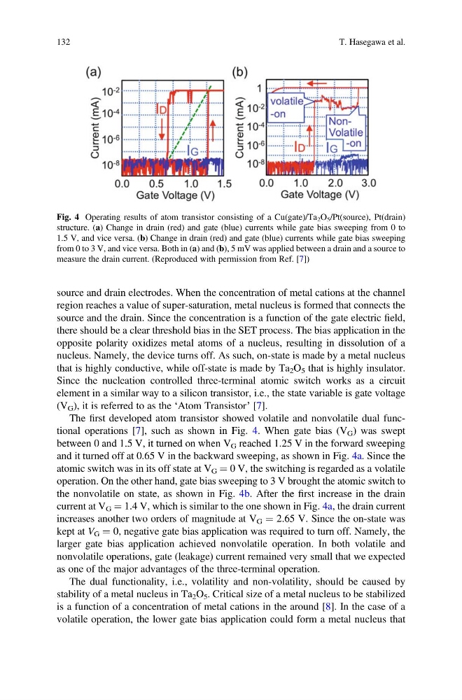
The first developed atom transistor showed volatile and nonvolatile dual functional operations [7], such as shown in Fig. 4. When gate bias (V G ) was swept
between 0 and 1.5 V, it turned on when V G reached 1.25 V in the forward sweeping
and it turned off at 0.65 V in the backward sweeping, as shown in Fig. 4a. Since the
atomic switch was in its off state at V G ¼ 0 V, the switching is regarded as a volatile
operation. On the other hand, gate bias sweeping to 3 V brought the atomic switch to
the nonvolatile on state, as shown in Fig. 4b. After the first increase in the drain
current at V G ¼ 1.4 V, which is similar to the one shown in Fig. 4a, the drain current
increases another two orders of magnitude at V G ¼ 2.65 V. Since the on-state was
kept at V G ¼ 0, negative gate bias application was required to turn off. Namely, the
larger gate bias application achieved nonvolatile operation. In both volatile and
nonvolatile operations, gate (leakage) current remained very small that we expected
as one of the major advantages of the three-terminal operation.
The dual functionality, i.e., volatility and non-volatility, should be caused by
stability of a metal nucleus in Ta 2 O 5 . Critical size of a metal nucleus to be stabilized
is a function of a concentration of metal cations in the around [8]. In the case of a
volatile operation, the lower gate bias application could form a metal nucleus that
Fig. 4 Operating results of atom transistor consisting of a Cu(gate)/Ta 2 O 5 /Pt(source), Pt(drain)
structure. (a) Change in drain (red) and gate (blue) currents while gate bias sweeping from 0 to
1.5 V, and vice versa. (b) Change in drain (red) and gate (blue) currents while gate bias sweeping
from 0 to 3 V, and vice versa. Both in (a) and (b), 5 mV was applied between a drain and a source to
measure the drain current. (Reproduced with permission from Ref. [7])
132
T. Hasegawa et al.
region reaches a value of super-saturation, metal nucleus is formed that connects the
source and the drain. Since the concentration is a function of the gate electric field,
there should be a clear threshold bias in the SET process. The bias application in the
opposite polarity oxidizes metal atoms of a nucleus, resulting in dissolution of a
nucleus. Namely, the device turns off. As such, on-state is made by a metal nucleus
that is highly conductive, while off-state is made by Ta 2 O 5 that is highly insulator.
Since the nucleation controlled three-terminal atomic switch works as a circuit
element in a similar way to a silicon transistor, i.e., the state variable is gate voltage
(V G ), it is referred to as the ‘Atom Transistor’ [7].
The first developed atom transistor showed volatile and nonvolatile dual functional operations [7], such as shown in Fig. 4. When gate bias (V G ) was swept
between 0 and 1.5 V, it turned on when V G reached 1.25 V in the forward sweeping
and it turned off at 0.65 V in the backward sweeping, as shown in Fig. 4a. Since the
atomic switch was in its off state at V G ¼ 0 V, the switching is regarded as a volatile
operation. On the other hand, gate bias sweeping to 3 V brought the atomic switch to
the nonvolatile on state, as shown in Fig. 4b. After the first increase in the drain
current at V G ¼ 1.4 V, which is similar to the one shown in Fig. 4a, the drain current
increases another two orders of magnitude at V G ¼ 2.65 V. Since the on-state was
kept at V G ¼ 0, negative gate bias application was required to turn off. Namely, the
larger gate bias application achieved nonvolatile operation. In both volatile and
nonvolatile operations, gate (leakage) current remained very small that we expected
as one of the major advantages of the three-terminal operation.
The dual functionality, i.e., volatility and non-volatility, should be caused by
stability of a metal nucleus in Ta 2 O 5 . Critical size of a metal nucleus to be stabilized
is a function of a concentration of metal cations in the around [8]. In the case of a
volatile operation, the lower gate bias application could form a metal nucleus that
Fig. 4 Operating results of atom transistor consisting of a Cu(gate)/Ta 2 O 5 /Pt(source), Pt(drain)
structure. (a) Change in drain (red) and gate (blue) currents while gate bias sweeping from 0 to
1.5 V, and vice versa. (b) Change in drain (red) and gate (blue) currents while gate bias sweeping
from 0 to 3 V, and vice versa. Both in (a) and (b), 5 mV was applied between a drain and a source to
measure the drain current. (Reproduced with permission from Ref. [7])
132
T. Hasegawa et al.