

can exist while gate bias application. However, the decrease in a concentration of
metal cations in the around due to the backward sweeping of the gate bias dissolved a
nucleus. Namely, the size of a nucleus was not big enough. On the other hand, the
larger bias application made a size of a nucleus large enough, resulting in the
nonvolatile operation.
The gate bias used in the first demonstration of atom transistor was larger than
that of the conventional semiconductor transistors. Further reduction in the gate bias
was a big issue of the atom transistor to be overcome in order to compete with
semiconductor transistors. Our strategy was to reduce a gap size between a source
and a drain that should enable switching with the formation and annihilation of a
smaller metal nucleus, which is easily formed and dissolved with a smaller gate bias.
The gap size in the first demonstration was 10 nm.
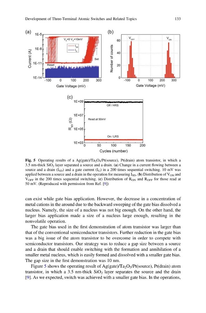
Figure 5 shows the operating result of Ag(gate)/Ta 2 O 5 /Pt(source), Pt(drain) atom
transistor, in which a 3.5 nm-thick SiO 2 layer separates the source and the drain
[9]. As we expected, switch was achieved with a smaller gate bias. In the operations,
Fig. 5 Operating results of a Ag(gate)/Ta 2 O 5 /Pt(source), Pt(drain) atom transistor, in which a
3.5 nm-thick SiO 2 layer separated a source and a drain. (a) Change in a current flowing between a
source and a drain (I SD ) and a gate current (I G ) in a 200 times sequential switching. 10 mV was
applied between a source and a drain in the operation for measuring I SD . (b) Distribution of V ON and
V OFF in the 200 times sequential switching. (c) Distribution of R ON and R OFF for those read at
50 mV. (Reproduced with permission from Ref. [9])
Development of Three-Terminal Atomic Switches and Related Topics
133
metal cations in the around due to the backward sweeping of the gate bias dissolved a
nucleus. Namely, the size of a nucleus was not big enough. On the other hand, the
larger bias application made a size of a nucleus large enough, resulting in the
nonvolatile operation.
The gate bias used in the first demonstration of atom transistor was larger than
that of the conventional semiconductor transistors. Further reduction in the gate bias
was a big issue of the atom transistor to be overcome in order to compete with
semiconductor transistors. Our strategy was to reduce a gap size between a source
and a drain that should enable switching with the formation and annihilation of a
smaller metal nucleus, which is easily formed and dissolved with a smaller gate bias.
The gap size in the first demonstration was 10 nm.
Figure 5 shows the operating result of Ag(gate)/Ta 2 O 5 /Pt(source), Pt(drain) atom
transistor, in which a 3.5 nm-thick SiO 2 layer separates the source and the drain
[9]. As we expected, switch was achieved with a smaller gate bias. In the operations,
Fig. 5 Operating results of a Ag(gate)/Ta 2 O 5 /Pt(source), Pt(drain) atom transistor, in which a
3.5 nm-thick SiO 2 layer separated a source and a drain. (a) Change in a current flowing between a
source and a drain (I SD ) and a gate current (I G ) in a 200 times sequential switching. 10 mV was
applied between a source and a drain in the operation for measuring I SD . (b) Distribution of V ON and
V OFF in the 200 times sequential switching. (c) Distribution of R ON and R OFF for those read at
50 mV. (Reproduced with permission from Ref. [9])
Development of Three-Terminal Atomic Switches and Related Topics
133