

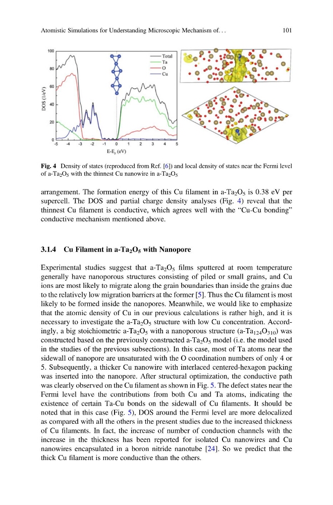
arrangement. The formation energy of this Cu filament in a-Ta 2 O 5 is 0.38 eV per
supercell. The DOS and partial charge density analyses (Fig. 4) reveal that the
thinnest Cu filament is conductive, which agrees well with the “Cu-Cu bonding”
conductive mechanism mentioned above.
3.1.4 Cu Filament in a-Ta 2 O 5 with Nanopore
Experimental studies suggest that a-Ta 2 O 5 films sputtered at room temperature
generally have nanoporous structures consisting of piled or small grains, and Cu
ions are most likely to migrate along the grain boundaries than inside the grains due
to the relatively low migration barriers at the former [5]. Thus the Cu filament is most
likely to be formed inside the nanopores. Meanwhile, we would like to emphasize
that the atomic density of Cu in our previous calculations is rather high, and it is
necessary to investigate the a-Ta 2 O 5 structure with low Cu concentration. Accordingly, a big stoichiometric a-Ta 2 O 5 with a nanoporous structure (a-Ta 124 O 310 ) was
constructed based on the previously constructed a-Ta 2 O 5 model (i.e. the model used
in the studies of the previous subsections). In this case, most of Ta atoms near the
sidewall of nanopore are unsaturated with the O coordination numbers of only 4 or
5. Subsequently, a thicker Cu nanowire with interlaced centered-hexagon packing
was inserted into the nanopore. After structural optimization, the conductive path
was clearly observed on the Cu filament as shown in Fig. 5. The defect states near the
Fermi level have the contributions from both Cu and Ta atoms, indicating the
existence of certain Ta-Cu bonds on the sidewall of Cu filaments. It should be
noted that in this case (Fig. 5), DOS around the Fermi level are more delocalized
as compared with all the others in the present studies due to the increased thickness
of Cu filaments. In fact, the increase of number of conduction channels with the
increase in the thickness has been reported for isolated Cu nanowires and Cu
nanowires encapsulated in a boron nitride nanotube [24]. So we predict that the
thick Cu filament is more conductive than the others.
Fig. 4 Density of states (reproduced from Ref. [6]) and local density of states near the Fermi level
of a-Ta 2 O 5 with the thinnest Cu nanowire in a-Ta 2 O 5
Atomistic Simulations for Understanding Microscopic Mechanism of. . .
101
supercell. The DOS and partial charge density analyses (Fig. 4) reveal that the
thinnest Cu filament is conductive, which agrees well with the “Cu-Cu bonding”
conductive mechanism mentioned above.
3.1.4 Cu Filament in a-Ta 2 O 5 with Nanopore
Experimental studies suggest that a-Ta 2 O 5 films sputtered at room temperature
generally have nanoporous structures consisting of piled or small grains, and Cu
ions are most likely to migrate along the grain boundaries than inside the grains due
to the relatively low migration barriers at the former [5]. Thus the Cu filament is most
likely to be formed inside the nanopores. Meanwhile, we would like to emphasize
that the atomic density of Cu in our previous calculations is rather high, and it is
necessary to investigate the a-Ta 2 O 5 structure with low Cu concentration. Accordingly, a big stoichiometric a-Ta 2 O 5 with a nanoporous structure (a-Ta 124 O 310 ) was
constructed based on the previously constructed a-Ta 2 O 5 model (i.e. the model used
in the studies of the previous subsections). In this case, most of Ta atoms near the
sidewall of nanopore are unsaturated with the O coordination numbers of only 4 or
5. Subsequently, a thicker Cu nanowire with interlaced centered-hexagon packing
was inserted into the nanopore. After structural optimization, the conductive path
was clearly observed on the Cu filament as shown in Fig. 5. The defect states near the
Fermi level have the contributions from both Cu and Ta atoms, indicating the
existence of certain Ta-Cu bonds on the sidewall of Cu filaments. It should be
noted that in this case (Fig. 5), DOS around the Fermi level are more delocalized
as compared with all the others in the present studies due to the increased thickness
of Cu filaments. In fact, the increase of number of conduction channels with the
increase in the thickness has been reported for isolated Cu nanowires and Cu
nanowires encapsulated in a boron nitride nanotube [24]. So we predict that the
thick Cu filament is more conductive than the others.
Fig. 4 Density of states (reproduced from Ref. [6]) and local density of states near the Fermi level
of a-Ta 2 O 5 with the thinnest Cu nanowire in a-Ta 2 O 5
Atomistic Simulations for Understanding Microscopic Mechanism of. . .
101