

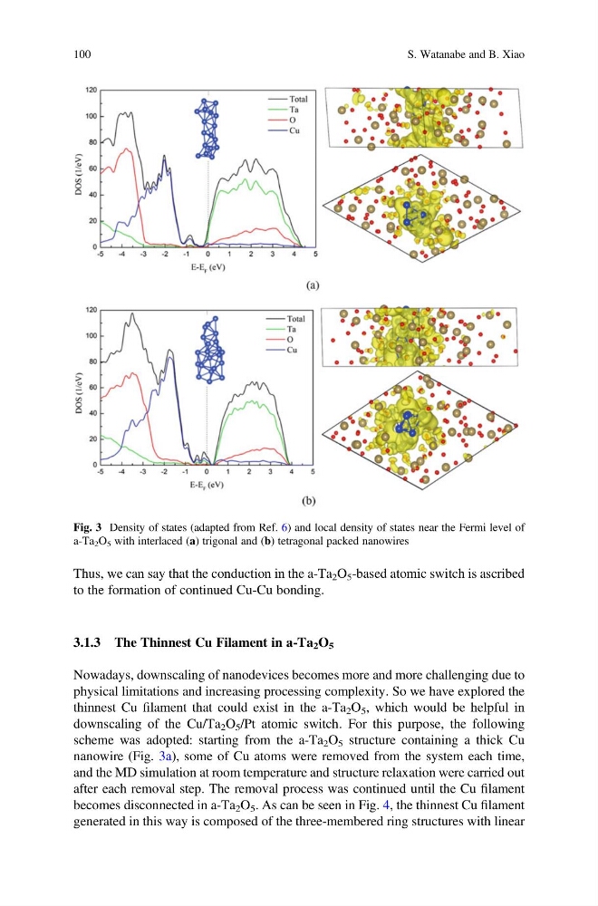
Thus, we can say that the conduction in the a-Ta 2 O 5 -based atomic switch is ascribed
to the formation of continued Cu-Cu bonding.
3.1.3 The Thinnest Cu Filament in a-Ta 2 O 5
Nowadays, downscaling of nanodevices becomes more and more challenging due to
physical limitations and increasing processing complexity. So we have explored the
thinnest Cu filament that could exist in the a-Ta 2 O 5 , which would be helpful in
downscaling of the Cu/Ta 2 O 5 /Pt atomic switch. For this purpose, the following
scheme was adopted: starting from the a-Ta 2 O 5 structure containing a thick Cu
nanowire (Fig. 3a), some of Cu atoms were removed from the system each time,
and the MD simulation at room temperature and structure relaxation were carried out
after each removal step. The removal process was continued until the Cu filament
becomes disconnected in a-Ta 2 O 5 . As can be seen in Fig. 4, the thinnest Cu filament
generated in this way is composed of the three-membered ring structures with linear
Fig. 3 Density of states (adapted from Ref. 6) and local density of states near the Fermi level of
a-Ta 2 O 5 with interlaced (a) trigonal and (b) tetragonal packed nanowires
100
S. Watanabe and B. Xiao
to the formation of continued Cu-Cu bonding.
3.1.3 The Thinnest Cu Filament in a-Ta 2 O 5
Nowadays, downscaling of nanodevices becomes more and more challenging due to
physical limitations and increasing processing complexity. So we have explored the
thinnest Cu filament that could exist in the a-Ta 2 O 5 , which would be helpful in
downscaling of the Cu/Ta 2 O 5 /Pt atomic switch. For this purpose, the following
scheme was adopted: starting from the a-Ta 2 O 5 structure containing a thick Cu
nanowire (Fig. 3a), some of Cu atoms were removed from the system each time,
and the MD simulation at room temperature and structure relaxation were carried out
after each removal step. The removal process was continued until the Cu filament
becomes disconnected in a-Ta 2 O 5 . As can be seen in Fig. 4, the thinnest Cu filament
generated in this way is composed of the three-membered ring structures with linear
Fig. 3 Density of states (adapted from Ref. 6) and local density of states near the Fermi level of
a-Ta 2 O 5 with interlaced (a) trigonal and (b) tetragonal packed nanowires
100
S. Watanabe and B. Xiao