

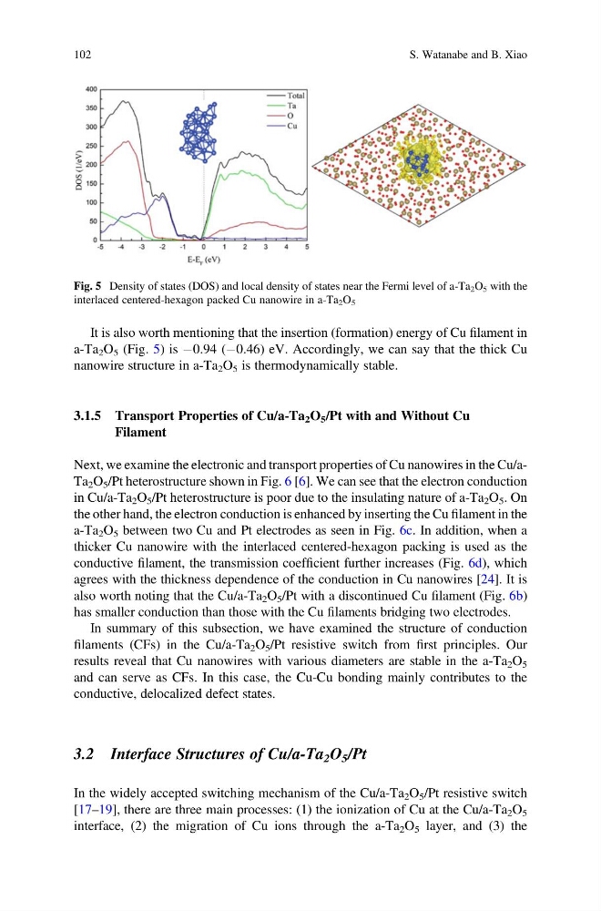
It is also worth mentioning that the insertion (formation) energy of Cu filament in
a-Ta 2 O 5 (Fig. 5) is À0.94 (À0.46) eV. Accordingly, we can say that the thick Cu
nanowire structure in a-Ta 2 O 5 is thermodynamically stable.
3.1.5 Transport Properties of Cu/a-Ta 2 O 5 /Pt with and Without Cu
Filament
Next, we examine the electronic and transport properties of Cu nanowires in the Cu/aTa 2 O 5 /Pt heterostructure shown in Fig. 6 [6]. We can see that the electron conduction
in Cu/a-Ta 2 O 5 /Pt heterostructure is poor due to the insulating nature of a-Ta 2 O 5 . On
the other hand, the electron conduction is enhanced by inserting the Cu filament in the
a-Ta 2 O 5 between two Cu and Pt electrodes as seen in Fig. 6c. In addition, when a
thicker Cu nanowire with the interlaced centered-hexagon packing is used as the
conductive filament, the transmission coefficient further increases (Fig. 6d), which
agrees with the thickness dependence of the conduction in Cu nanowires [24]. It is
also worth noting that the Cu/a-Ta 2 O 5 /Pt with a discontinued Cu filament (Fig. 6b)
has smaller conduction than those with the Cu filaments bridging two electrodes.
In summary of this subsection, we have examined the structure of conduction
filaments (CFs) in the Cu/a-Ta 2 O 5 /Pt resistive switch from first principles. Our
results reveal that Cu nanowires with various diameters are stable in the a-Ta 2 O 5
and can serve as CFs. In this case, the Cu-Cu bonding mainly contributes to the
conductive, delocalized defect states.
3.2 Interface Structures of Cu/a-Ta 2 O 5 /Pt
In the widely accepted switching mechanism of the Cu/a-Ta 2 O 5 /Pt resistive switch
[17–19], there are three main processes: (1) the ionization of Cu at the Cu/a-Ta 2 O 5
interface, (2) the migration of Cu ions through the a-Ta 2 O 5 layer, and (3) the
Fig. 5 Density of states (DOS) and local density of states near the Fermi level of a-Ta 2 O 5 with the
interlaced centered-hexagon packed Cu nanowire in a-Ta 2 O 5
102
S. Watanabe and B. Xiao
a-Ta 2 O 5 (Fig. 5) is À0.94 (À0.46) eV. Accordingly, we can say that the thick Cu
nanowire structure in a-Ta 2 O 5 is thermodynamically stable.
3.1.5 Transport Properties of Cu/a-Ta 2 O 5 /Pt with and Without Cu
Filament
Next, we examine the electronic and transport properties of Cu nanowires in the Cu/aTa 2 O 5 /Pt heterostructure shown in Fig. 6 [6]. We can see that the electron conduction
in Cu/a-Ta 2 O 5 /Pt heterostructure is poor due to the insulating nature of a-Ta 2 O 5 . On
the other hand, the electron conduction is enhanced by inserting the Cu filament in the
a-Ta 2 O 5 between two Cu and Pt electrodes as seen in Fig. 6c. In addition, when a
thicker Cu nanowire with the interlaced centered-hexagon packing is used as the
conductive filament, the transmission coefficient further increases (Fig. 6d), which
agrees with the thickness dependence of the conduction in Cu nanowires [24]. It is
also worth noting that the Cu/a-Ta 2 O 5 /Pt with a discontinued Cu filament (Fig. 6b)
has smaller conduction than those with the Cu filaments bridging two electrodes.
In summary of this subsection, we have examined the structure of conduction
filaments (CFs) in the Cu/a-Ta 2 O 5 /Pt resistive switch from first principles. Our
results reveal that Cu nanowires with various diameters are stable in the a-Ta 2 O 5
and can serve as CFs. In this case, the Cu-Cu bonding mainly contributes to the
conductive, delocalized defect states.
3.2 Interface Structures of Cu/a-Ta 2 O 5 /Pt
In the widely accepted switching mechanism of the Cu/a-Ta 2 O 5 /Pt resistive switch
[17–19], there are three main processes: (1) the ionization of Cu at the Cu/a-Ta 2 O 5
interface, (2) the migration of Cu ions through the a-Ta 2 O 5 layer, and (3) the
Fig. 5 Density of states (DOS) and local density of states near the Fermi level of a-Ta 2 O 5 with the
interlaced centered-hexagon packed Cu nanowire in a-Ta 2 O 5
102
S. Watanabe and B. Xiao