

6.3 ReConfigurable CAM Extension to CMOS
87
1,E-11
1,E-10
1,E-09
1,E-08
1,E-07
0,35 0,45 0,55 0,65 0,75 0,85 0,95
WLPulse_min Read
WLPulse_min Write
10 -11
10 -10
10 -9
10 -8
10 -7
Supply Voltage[V]
WLPulse_min [s]
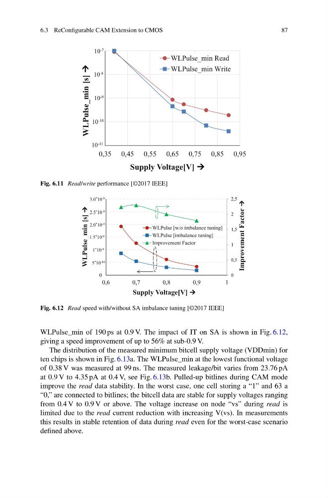
Fig. 6.11 Read/write performance [©2017 IEEE]
0
0,5
1
1,5
2
2,5
0,E+00
5,E-10
1,E-09
2,E-09
2,E-09
3,E-09
3,E-09
0,6
0,7
0,8
0,9
1
WLPulse [w/o imbalance tuning]
WLPulse [imbalance tuning]
Improvement Factor
0
Supply Voltage[V]
WLPulse_min [s]
Improvement Factor
5 * 10 -10
1 * 10 -9
1.5 * 10 -9
2.0 * 10 -9
2.5 * 10 -9
3.0 * 10 -9
Fig. 6.12 Read speed with/without SA imbalance tuning [©2017 IEEE]
WLPulse_min of 190 ps at 0.9 V. The impact of IT on SA is shown in Fig. 6.12,
giving a speed improvement of up to 56% at sub-0.9 V.
The distribution of the measured minimum bitcell supply voltage (VDDmin) for
ten chips is shown in Fig. 6.13a. The WLPulse_min at the lowest functional voltage
of 0.38 V was measured at 99 ns. The measured leakage/bit varies from 23.76 pA
at 0.9 V to 4.35 pA at 0.4 V, see Fig. 6.13b. Pulled-up bitlines during CAM mode
improve the read data stability. In the worst case, one cell storing a “1” and 63 a
“0,” are connected to bitlines; the bitcell data are stable for supply voltages ranging
from 0.4 V to 0.9 V or above. The voltage increase on node “vs” during read is
limited due to the read current reduction with increasing V(vs). In measurements
this results in stable retention of data during read even for the worst-case scenario
defined above.
87
1,E-11
1,E-10
1,E-09
1,E-08
1,E-07
0,35 0,45 0,55 0,65 0,75 0,85 0,95
WLPulse_min Read
WLPulse_min Write
10 -11
10 -10
10 -9
10 -8
10 -7
Supply Voltage[V]
WLPulse_min [s]
Fig. 6.11 Read/write performance [©2017 IEEE]
0
0,5
1
1,5
2
2,5
0,E+00
5,E-10
1,E-09
2,E-09
2,E-09
3,E-09
3,E-09
0,6
0,7
0,8
0,9
1
WLPulse [w/o imbalance tuning]
WLPulse [imbalance tuning]
Improvement Factor
0
Supply Voltage[V]
WLPulse_min [s]
Improvement Factor
5 * 10 -10
1 * 10 -9
1.5 * 10 -9
2.0 * 10 -9
2.5 * 10 -9
3.0 * 10 -9
Fig. 6.12 Read speed with/without SA imbalance tuning [©2017 IEEE]
WLPulse_min of 190 ps at 0.9 V. The impact of IT on SA is shown in Fig. 6.12,
giving a speed improvement of up to 56% at sub-0.9 V.
The distribution of the measured minimum bitcell supply voltage (VDDmin) for
ten chips is shown in Fig. 6.13a. The WLPulse_min at the lowest functional voltage
of 0.38 V was measured at 99 ns. The measured leakage/bit varies from 23.76 pA
at 0.9 V to 4.35 pA at 0.4 V, see Fig. 6.13b. Pulled-up bitlines during CAM mode
improve the read data stability. In the worst case, one cell storing a “1” and 63 a
“0,” are connected to bitlines; the bitcell data are stable for supply voltages ranging
from 0.4 V to 0.9 V or above. The voltage increase on node “vs” during read is
limited due to the read current reduction with increasing V(vs). In measurements
this results in stable retention of data during read even for the worst-case scenario
defined above.