

86
6 Content-Addressable Memories
6.3.1.2 Pseudo-Ternary CAM (TCAM) Mode
The pseudo-TCAM Mode differs from the binary mode in the following aspect: in a
CAM search both wordlines can be left low for a row in order to mask the bits of that
row in a search operation. This can be used to implement a global-mask operation,
which is used in routing applications. The global mask can be implemented as a
configuration register or it can be obtained from another SRAM storage [80].
6.3.1.3 SRAM Mode
In SRAM mode a read is performed using “vs” with just wl1 high for a single
row, working as address selection for read. The write operation in SRAM mode is
performed in the conventional way using bitlines as complementary data lines and
both wordlines high for a single row acting as address selection.
6.3.2 Measured Results
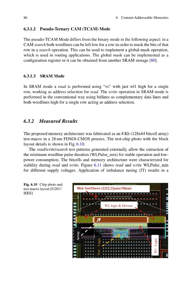
The proposed memory architecture was fabricated as an 8 Kb (128x64 bitcell array)
test-macro in a 28 nm FDSOI-CMOS process. The test-chip photo with the block
layout details is shown in Fig. 6.10.
The read/write/search test patterns generated externally allow the extraction of
the minimum wordline pulse duration (WLPulse_min) for stable operation and lowpower consumption. The bitcells and memory architecture were characterized for
stability during read and write. Figure 6.11 shows read and write WLPulse_min
for different supply voltages. Application of imbalance tuning (IT) results in a
Fig. 6.10 Chip photo and
test-macro layout [©2017
IEEE]
Test
- Logic
IO - Logic
Array
WL logic & Drivers
8Kb-TestMacro (2222.22μmx150μm)
6 Content-Addressable Memories
6.3.1.2 Pseudo-Ternary CAM (TCAM) Mode
The pseudo-TCAM Mode differs from the binary mode in the following aspect: in a
CAM search both wordlines can be left low for a row in order to mask the bits of that
row in a search operation. This can be used to implement a global-mask operation,
which is used in routing applications. The global mask can be implemented as a
configuration register or it can be obtained from another SRAM storage [80].
6.3.1.3 SRAM Mode
In SRAM mode a read is performed using “vs” with just wl1 high for a single
row, working as address selection for read. The write operation in SRAM mode is
performed in the conventional way using bitlines as complementary data lines and
both wordlines high for a single row acting as address selection.
6.3.2 Measured Results
The proposed memory architecture was fabricated as an 8 Kb (128x64 bitcell array)
test-macro in a 28 nm FDSOI-CMOS process. The test-chip photo with the block
layout details is shown in Fig. 6.10.
The read/write/search test patterns generated externally allow the extraction of
the minimum wordline pulse duration (WLPulse_min) for stable operation and lowpower consumption. The bitcells and memory architecture were characterized for
stability during read and write. Figure 6.11 shows read and write WLPulse_min
for different supply voltages. Application of imbalance tuning (IT) results in a
Fig. 6.10 Chip photo and
test-macro layout [©2017
IEEE]
Test
- Logic
IO - Logic
Array
WL logic & Drivers
8Kb-TestMacro (2222.22μmx150μm)