

6.3 ReConfigurable CAM Extension to CMOS
85
RD_EN
wl
vs[0]
vs[1]
SAQb[0]
SAQ[1]
DQ[1]
DQ[0]
SAEN
SAEN
SAQb[0]
SAQ[0]
SAQ[1]
SAQb[1]
1.0
0.8
0.6
0.4
0.2
0.0
1.0
0.8
0.6
0.4
0.2
0.0
1.0
1.0
1.0
1.0
0.8
0.6
0.4
0.2
0.0
0.9
0.8
0.7
0.6
0.5
0.4
0.3
0.2
0.1
0.0
0.6
0.3
0.0
0.8
0.6
0.4
0.2
0.0
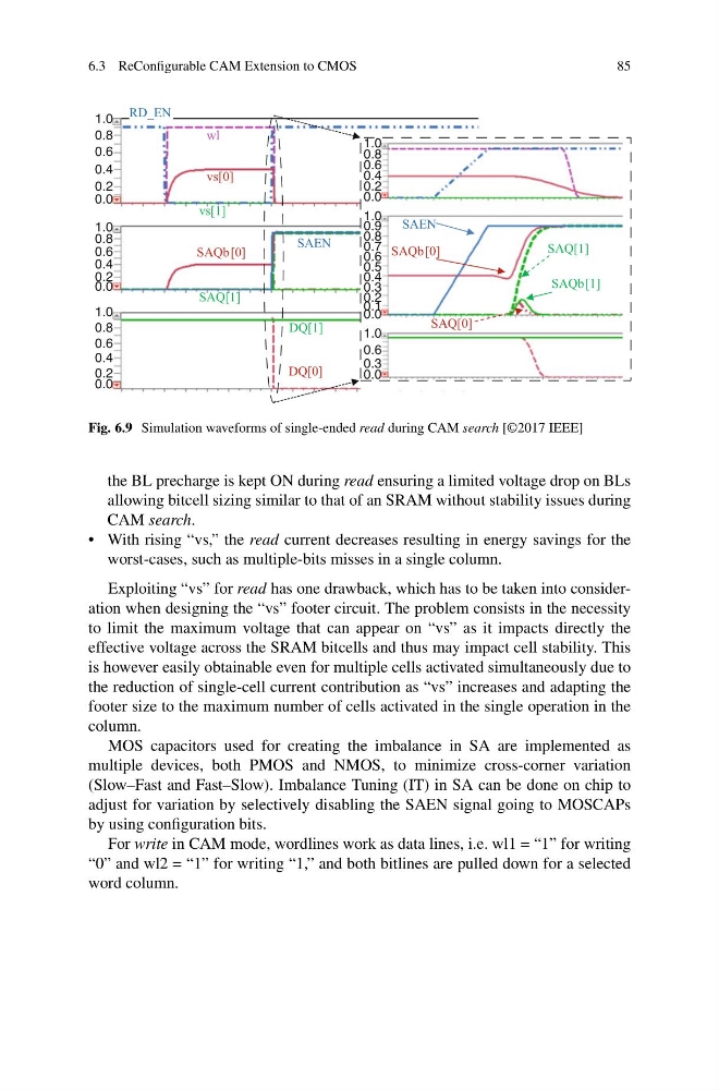
Fig. 6.9 Simulation waveforms of single-ended read during CAM search [©2017 IEEE]
the BL precharge is kept ON during read ensuring a limited voltage drop on BLs
allowing bitcell sizing similar to that of an SRAM without stability issues during
CAM search.
• With rising “vs,” the read current decreases resulting in energy savings for the
worst-cases, such as multiple-bits misses in a single column.
Exploiting “vs” for read has one drawback, which has to be taken into consideration when designing the “vs” footer circuit. The problem consists in the necessity
to limit the maximum voltage that can appear on “vs” as it impacts directly the
effective voltage across the SRAM bitcells and thus may impact cell stability. This
is however easily obtainable even for multiple cells activated simultaneously due to
the reduction of single-cell current contribution as “vs” increases and adapting the
footer size to the maximum number of cells activated in the single operation in the
column.
MOS capacitors used for creating the imbalance in SA are implemented as
multiple devices, both PMOS and NMOS, to minimize cross-corner variation
(Slow–Fast and Fast–Slow). Imbalance Tuning (IT) in SA can be done on chip to
adjust for variation by selectively disabling the SAEN signal going to MOSCAPs
by using configuration bits.
For write in CAM mode, wordlines work as data lines, i.e. wl1 = “1” for writing
“0” and wl2 = “1” for writing “1,” and both bitlines are pulled down for a selected
word column.
85
RD_EN
wl
vs[0]
vs[1]
SAQb[0]
SAQ[1]
DQ[1]
DQ[0]
SAEN
SAEN
SAQb[0]
SAQ[0]
SAQ[1]
SAQb[1]
1.0
0.8
0.6
0.4
0.2
0.0
1.0
0.8
0.6
0.4
0.2
0.0
1.0
1.0
1.0
1.0
0.8
0.6
0.4
0.2
0.0
0.9
0.8
0.7
0.6
0.5
0.4
0.3
0.2
0.1
0.0
0.6
0.3
0.0
0.8
0.6
0.4
0.2
0.0
Fig. 6.9 Simulation waveforms of single-ended read during CAM search [©2017 IEEE]
the BL precharge is kept ON during read ensuring a limited voltage drop on BLs
allowing bitcell sizing similar to that of an SRAM without stability issues during
CAM search.
• With rising “vs,” the read current decreases resulting in energy savings for the
worst-cases, such as multiple-bits misses in a single column.
Exploiting “vs” for read has one drawback, which has to be taken into consideration when designing the “vs” footer circuit. The problem consists in the necessity
to limit the maximum voltage that can appear on “vs” as it impacts directly the
effective voltage across the SRAM bitcells and thus may impact cell stability. This
is however easily obtainable even for multiple cells activated simultaneously due to
the reduction of single-cell current contribution as “vs” increases and adapting the
footer size to the maximum number of cells activated in the single operation in the
column.
MOS capacitors used for creating the imbalance in SA are implemented as
multiple devices, both PMOS and NMOS, to minimize cross-corner variation
(Slow–Fast and Fast–Slow). Imbalance Tuning (IT) in SA can be done on chip to
adjust for variation by selectively disabling the SAEN signal going to MOSCAPs
by using configuration bits.
For write in CAM mode, wordlines work as data lines, i.e. wl1 = “1” for writing
“0” and wl2 = “1” for writing “1,” and both bitlines are pulled down for a selected
word column.