

84
6 Content-Addressable Memories
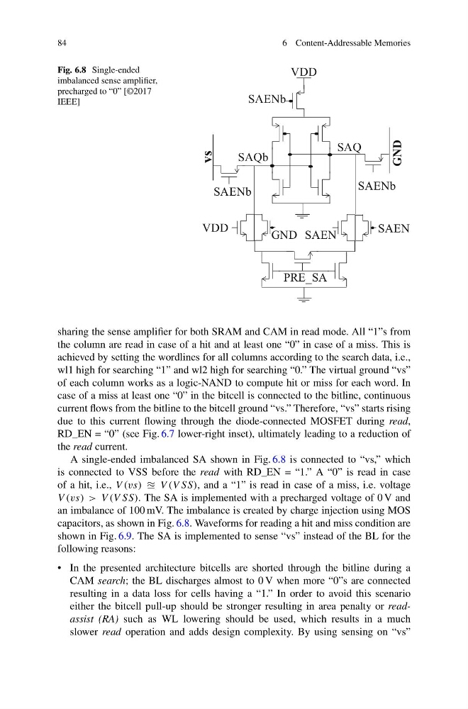
Fig. 6.8 Single-ended
imbalanced sense amplifier,
precharged to “0” [©2017
IEEE]
VDD
VDD
SAEN
SAENb
GND
SAENb
SAENb
vs
SAEN
GND
PRE_SA
SAQb
SAQ
sharing the sense amplifier for both SRAM and CAM in read mode. All “1”s from
the column are read in case of a hit and at least one “0” in case of a miss. This is
achieved by setting the wordlines for all columns according to the search data, i.e.,
wl1 high for searching “1” and wl2 high for searching “0.” The virtual ground “vs”
of each column works as a logic-NAND to compute hit or miss for each word. In
case of a miss at least one “0” in the bitcell is connected to the bitline, continuous
current flows from the bitline to the bitcell ground “vs.” Therefore, “vs” starts rising
due to this current flowing through the diode-connected MOSFET during read,
RD_EN = “0” (see Fig. 6.7 lower-right inset), ultimately leading to a reduction of
the read current.
A single-ended imbalanced SA shown in Fig. 6.8 is connected to “vs,” which
is connected to VSS before the read with RD_EN = “1.” A “0” is read in case
of a hit, i.e., V (vs) V (V SS), and a “1” is read in case of a miss, i.e. voltage
V (vs) > V (V SS). The SA is implemented with a precharged voltage of 0 V and
an imbalance of 100 mV. The imbalance is created by charge injection using MOS
capacitors, as shown in Fig. 6.8. Waveforms for reading a hit and miss condition are
shown in Fig. 6.9. The SA is implemented to sense “vs” instead of the BL for the
following reasons:
• In the presented architecture bitcells are shorted through the bitline during a
CAM search; the BL discharges almost to 0 V when more “0”s are connected
resulting in a data loss for cells having a “1.” In order to avoid this scenario
either the bitcell pull-up should be stronger resulting in area penalty or readassist (RA) such as WL lowering should be used, which results in a much
slower read operation and adds design complexity. By using sensing on “vs”
6 Content-Addressable Memories
Fig. 6.8 Single-ended
imbalanced sense amplifier,
precharged to “0” [©2017
IEEE]
VDD
VDD
SAEN
SAENb
GND
SAENb
SAENb
vs
SAEN
GND
PRE_SA
SAQb
SAQ
sharing the sense amplifier for both SRAM and CAM in read mode. All “1”s from
the column are read in case of a hit and at least one “0” in case of a miss. This is
achieved by setting the wordlines for all columns according to the search data, i.e.,
wl1 high for searching “1” and wl2 high for searching “0.” The virtual ground “vs”
of each column works as a logic-NAND to compute hit or miss for each word. In
case of a miss at least one “0” in the bitcell is connected to the bitline, continuous
current flows from the bitline to the bitcell ground “vs.” Therefore, “vs” starts rising
due to this current flowing through the diode-connected MOSFET during read,
RD_EN = “0” (see Fig. 6.7 lower-right inset), ultimately leading to a reduction of
the read current.
A single-ended imbalanced SA shown in Fig. 6.8 is connected to “vs,” which
is connected to VSS before the read with RD_EN = “1.” A “0” is read in case
of a hit, i.e., V (vs) V (V SS), and a “1” is read in case of a miss, i.e. voltage
V (vs) > V (V SS). The SA is implemented with a precharged voltage of 0 V and
an imbalance of 100 mV. The imbalance is created by charge injection using MOS
capacitors, as shown in Fig. 6.8. Waveforms for reading a hit and miss condition are
shown in Fig. 6.9. The SA is implemented to sense “vs” instead of the BL for the
following reasons:
• In the presented architecture bitcells are shorted through the bitline during a
CAM search; the BL discharges almost to 0 V when more “0”s are connected
resulting in a data loss for cells having a “1.” In order to avoid this scenario
either the bitcell pull-up should be stronger resulting in area penalty or readassist (RA) such as WL lowering should be used, which results in a much
slower read operation and adds design complexity. By using sensing on “vs”