

80
6 Content-Addressable Memories
0.6
0.7
0.8
0.9
1
SRAM RD-256 bits/row
SRAM RD-128 bits/row
SRAM RD-64 bits/row
SRAM RD-128 bits/row with RA
WR with WA
SRAM RD-32 bits/row
Write (WR)
SRAM RD-256 bits/row with RA
CAM Rd-256 bits/col
CAM RD-128 bits/col
CAM RD-128 bits/col with RA
0.E+00
2.E-09
4.E-09
6.E-09
8.E-09
1.E-08
1.E-08
1.E-08
2.E-08
2.E-08
2.E-08
0.6
0.7
0.8
0.9
1
SRAM RD-256 bits/row
WR with WA
CAM RD-128 bits/col with RA
2.E-10
7.E-10
1.E-09
2.E-09
0.8
0.9
1
700
60
50
40
30
20
10
0
0
2
4
6
8
10
12
14
16
18
20
1.7
1.2
0.7
0.2
P
L
W
min
]
s
n
[
Supply Voltage [V]
WLP
min [ns]
Supply Voltage [V]
Configuration
128 bits/column
256 bits/row
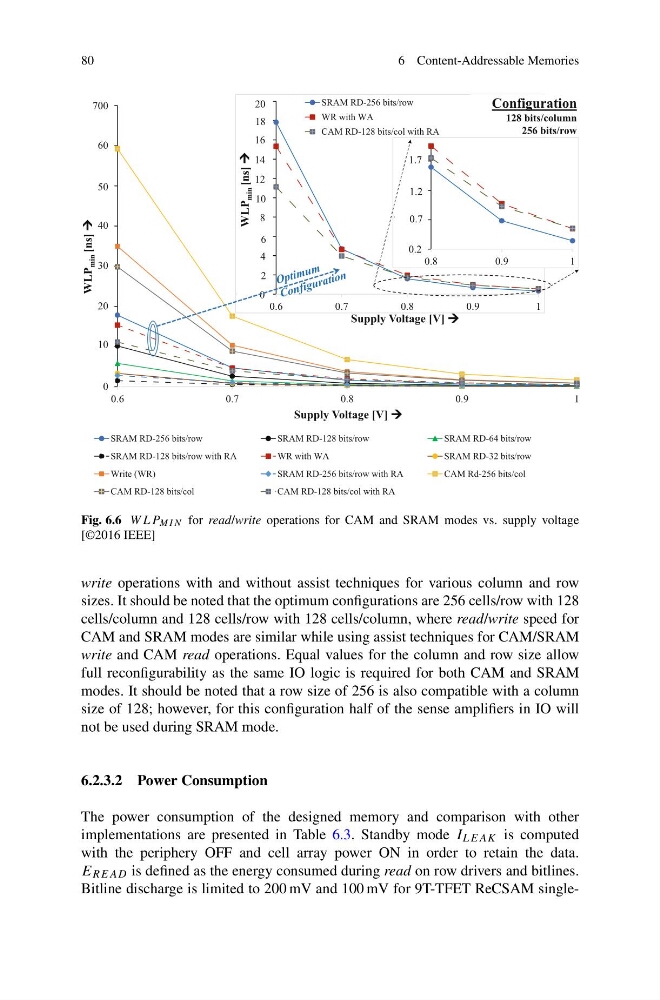
Fig. 6.6 W LP MI N for read/write operations for CAM and SRAM modes vs. supply voltage
[©2016 IEEE]
write operations with and without assist techniques for various column and row
sizes. It should be noted that the optimum configurations are 256 cells/row with 128
cells/column and 128 cells/row with 128 cells/column, where read/write speed for
CAM and SRAM modes are similar while using assist techniques for CAM/SRAM
write and CAM read operations. Equal values for the column and row size allow
full reconfigurability as the same IO logic is required for both CAM and SRAM
modes. It should be noted that a row size of 256 is also compatible with a column
size of 128; however, for this configuration half of the sense amplifiers in IO will
not be used during SRAM mode.
6.2.3.2 Power Consumption
The power consumption of the designed memory and comparison with other
implementations are presented in Table 6.3. Standby mode I LEAK is computed
with the periphery OFF and cell array power ON in order to retain the data.
E READ is defined as the energy consumed during read on row drivers and bitlines.
Bitline discharge is limited to 200 mV and 100 mV for 9T-TFET ReCSAM single-
6 Content-Addressable Memories
0.6
0.7
0.8
0.9
1
SRAM RD-256 bits/row
SRAM RD-128 bits/row
SRAM RD-64 bits/row
SRAM RD-128 bits/row with RA
WR with WA
SRAM RD-32 bits/row
Write (WR)
SRAM RD-256 bits/row with RA
CAM Rd-256 bits/col
CAM RD-128 bits/col
CAM RD-128 bits/col with RA
0.E+00
2.E-09
4.E-09
6.E-09
8.E-09
1.E-08
1.E-08
1.E-08
2.E-08
2.E-08
2.E-08
0.6
0.7
0.8
0.9
1
SRAM RD-256 bits/row
WR with WA
CAM RD-128 bits/col with RA
2.E-10
7.E-10
1.E-09
2.E-09
0.8
0.9
1
700
60
50
40
30
20
10
0
0
2
4
6
8
10
12
14
16
18
20
1.7
1.2
0.7
0.2
P
L
W
min
]
s
n
[
Supply Voltage [V]
WLP
min [ns]
Supply Voltage [V]
Configuration
128 bits/column
256 bits/row
Fig. 6.6 W LP MI N for read/write operations for CAM and SRAM modes vs. supply voltage
[©2016 IEEE]
write operations with and without assist techniques for various column and row
sizes. It should be noted that the optimum configurations are 256 cells/row with 128
cells/column and 128 cells/row with 128 cells/column, where read/write speed for
CAM and SRAM modes are similar while using assist techniques for CAM/SRAM
write and CAM read operations. Equal values for the column and row size allow
full reconfigurability as the same IO logic is required for both CAM and SRAM
modes. It should be noted that a row size of 256 is also compatible with a column
size of 128; however, for this configuration half of the sense amplifiers in IO will
not be used during SRAM mode.
6.2.3.2 Power Consumption
The power consumption of the designed memory and comparison with other
implementations are presented in Table 6.3. Standby mode I LEAK is computed
with the periphery OFF and cell array power ON in order to retain the data.
E READ is defined as the energy consumed during read on row drivers and bitlines.
Bitline discharge is limited to 200 mV and 100 mV for 9T-TFET ReCSAM single-