

6.2 Hybrid TFET Reconfigurable CAM/SRAM Array Based on a 9T-TFET. . .
79
VDD
BLL[0]
BLR[1]
BLR[0]
RBL
BLL[1]
GND
WL2
WL1
VDD
GND
Bitcell-0
Bitcell-1
Size-Cell Array
96.62x63.59 μm 2
Bitcell Area (logic design rules)
0.375 μm 2
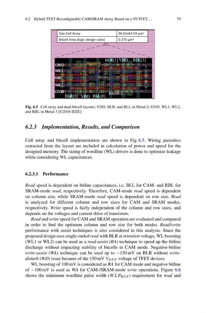
Fig. 6.5 Cell array and dual-bitcell layouts; VDD, BLR, and BLL in Metal-2; GND, WL1, WL2,
and RBL in Metal-3 [©2016 IEEE]
6.2.3 Implementation, Results, and Comparison
Cell array and bitcell implementation are shown in Fig. 6.5. Wiring parasitics
extracted from the layout are included in calculation of power and speed for the
designed memory. The sizing of wordline (WL) drivers is done to optimize leakage
while considering WL capacitances.
6.2.3.1 Performance
Read speed is dependent on bitline capacitances, i.e. BLL for CAM- and RBL for
SRAM-mode read, respectively. Therefore, CAM-mode read speed is dependent
on column size, while SRAM-mode read speed is dependent on row size. Read
is analyzed for different column and row sizes for CAM and SRAM modes,
respectively. Write speed is fairly independent of the column and row sizes, and
depends on the voltages and current drive of transistors.
Read and write speed for CAM and SRAM operation are evaluated and compared
in order to find the optimum column and row size for both modes. Read/write
performance with assist techniques is also considered in this analysis. Since the
proposed design uses single-ended read with BLR at retention voltage, WL boosting
(WL1 or WL2) can be used as a read-assist (RA) technique to speed up the bitline
discharge without impacting stability of bitcells in CAM mode. Negative-bitline
write-assist (WA) technique can be used up to −150 mV on BLR without writedisturb (WD) issue because of the 150 mV V OF F voltage of TFET devices.
WL boosting of 100 mV is considered as RA for CAM mode and negative bitline
of −100 mV is used as WA for CAM-/SRAM-mode write operations. Figure 6.6
shows the minimum wordline pulse width (W LP MI N ) requirement for read and
79
VDD
BLL[0]
BLR[1]
BLR[0]
RBL
BLL[1]
GND
WL2
WL1
VDD
GND
Bitcell-0
Bitcell-1
Size-Cell Array
96.62x63.59 μm 2
Bitcell Area (logic design rules)
0.375 μm 2
Fig. 6.5 Cell array and dual-bitcell layouts; VDD, BLR, and BLL in Metal-2; GND, WL1, WL2,
and RBL in Metal-3 [©2016 IEEE]
6.2.3 Implementation, Results, and Comparison
Cell array and bitcell implementation are shown in Fig. 6.5. Wiring parasitics
extracted from the layout are included in calculation of power and speed for the
designed memory. The sizing of wordline (WL) drivers is done to optimize leakage
while considering WL capacitances.
6.2.3.1 Performance
Read speed is dependent on bitline capacitances, i.e. BLL for CAM- and RBL for
SRAM-mode read, respectively. Therefore, CAM-mode read speed is dependent
on column size, while SRAM-mode read speed is dependent on row size. Read
is analyzed for different column and row sizes for CAM and SRAM modes,
respectively. Write speed is fairly independent of the column and row sizes, and
depends on the voltages and current drive of transistors.
Read and write speed for CAM and SRAM operation are evaluated and compared
in order to find the optimum column and row size for both modes. Read/write
performance with assist techniques is also considered in this analysis. Since the
proposed design uses single-ended read with BLR at retention voltage, WL boosting
(WL1 or WL2) can be used as a read-assist (RA) technique to speed up the bitline
discharge without impacting stability of bitcells in CAM mode. Negative-bitline
write-assist (WA) technique can be used up to −150 mV on BLR without writedisturb (WD) issue because of the 150 mV V OF F voltage of TFET devices.
WL boosting of 100 mV is considered as RA for CAM mode and negative bitline
of −100 mV is used as WA for CAM-/SRAM-mode write operations. Figure 6.6
shows the minimum wordline pulse width (W LP MI N ) requirement for read and