

78
6 Content-Addressable Memories
Table 6.2 Signal voltages during CAM- and SRAM-mode read [©2016 IEEE]
CAM mode
SRAM mode
Active cells (search
data = “1”)
Active cells (search
data = “0”)
Cell read (active
column)
Unselected
columns
BLL
(precharge
voltage)
1 V
1 V
1 V
1 V
RBL
(precharge
voltage)
1 V
1 V
1 V
1 V
BLR
0.6 V
0.6 V
0 V
0.6 V
WL1
1 V
0 V
0 V
0 V
WL2
0 V
1 V
0 V
0 V
VDD
1 V
1 V
1 V
1 V
~550 ps
@128 bit word
V(WL1[0])
V(BLL[1])-CAM miss
V(BLL[0])-CAM hit
1.0
0.5
0.0
1.0
0.5
0.0
0
0.5n
1.0n
1.5n
2.0n
2.5n
3.0n
Time [s]
]
V
[
e
g
a
t
l
o
V
]
V
[
e
g
a
t
l
o
V
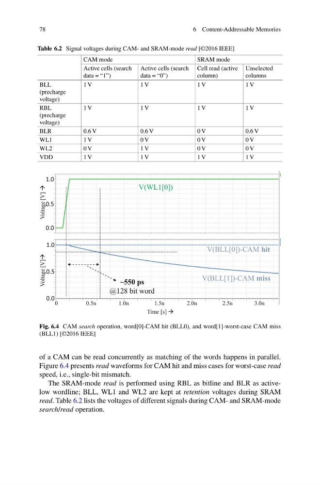
Fig. 6.4 CAM search operation, word[0]-CAM hit (BLL0), and word[1]-worst-case CAM miss
(BLL1) [©2016 IEEE]
of a CAM can be read concurrently as matching of the words happens in parallel.
Figure 6.4 presents read waveforms for CAM hit and miss cases for worst-case read
speed, i.e., single-bit mismatch.
The SRAM-mode read is performed using RBL as bitline and BLR as activelow wordline; BLL, WL1 and WL2 are kept at retention voltages during SRAM
read. Table 6.2 lists the voltages of different signals during CAM- and SRAM-mode
search/read operation.
6 Content-Addressable Memories
Table 6.2 Signal voltages during CAM- and SRAM-mode read [©2016 IEEE]
CAM mode
SRAM mode
Active cells (search
data = “1”)
Active cells (search
data = “0”)
Cell read (active
column)
Unselected
columns
BLL
(precharge
voltage)
1 V
1 V
1 V
1 V
RBL
(precharge
voltage)
1 V
1 V
1 V
1 V
BLR
0.6 V
0.6 V
0 V
0.6 V
WL1
1 V
0 V
0 V
0 V
WL2
0 V
1 V
0 V
0 V
VDD
1 V
1 V
1 V
1 V
~550 ps
@128 bit word
V(WL1[0])
V(BLL[1])-CAM miss
V(BLL[0])-CAM hit
1.0
0.5
0.0
1.0
0.5
0.0
0
0.5n
1.0n
1.5n
2.0n
2.5n
3.0n
Time [s]
]
V
[
e
g
a
t
l
o
V
]
V
[
e
g
a
t
l
o
V
Fig. 6.4 CAM search operation, word[0]-CAM hit (BLL0), and word[1]-worst-case CAM miss
(BLL1) [©2016 IEEE]
of a CAM can be read concurrently as matching of the words happens in parallel.
Figure 6.4 presents read waveforms for CAM hit and miss cases for worst-case read
speed, i.e., single-bit mismatch.
The SRAM-mode read is performed using RBL as bitline and BLR as activelow wordline; BLL, WL1 and WL2 are kept at retention voltages during SRAM
read. Table 6.2 lists the voltages of different signals during CAM- and SRAM-mode
search/read operation.