

6.2 Hybrid TFET Reconfigurable CAM/SRAM Array Based on a 9T-TFET. . .
77
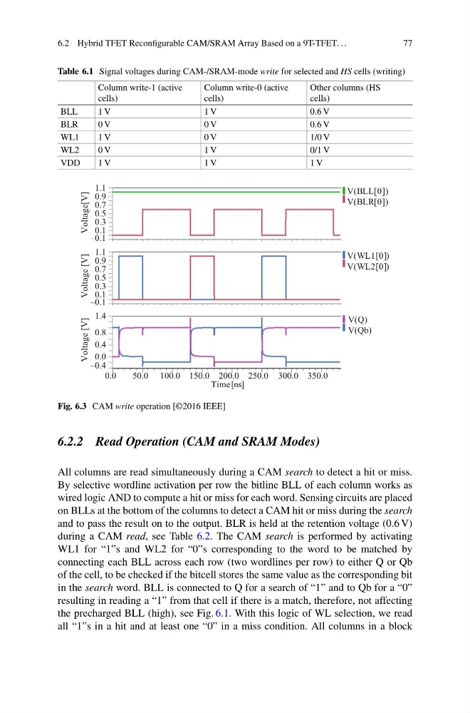
Table 6.1 Signal voltages during CAM-/SRAM-mode write for selected and HS cells (writing)
Column write-1 (active
cells)
Column write-0 (active
cells)
Other columns (HS
cells)
BLL
1 V
1 V
0.6 V
BLR
0 V
0 V
0.6 V
WL1
1 V
0 V
1/0 V
WL2
0 V
1 V
0/1 V
VDD
1 V
1 V
1 V
V(BLL[0])
V(BLR[0])
V(WL1[0])
V(WL2[0])
V(Q)
V(Qb)
Voltage [V]
Voltage[V]
Voltage [V]
Time [ns]
1.1
0.9
0.7
0.5
0.3
0.1
–0.1
1.1
0.9
0.7
0.5
0.3
0.1
1.4
0.8
0.4
0.0
0.0
50.0 100.0 150.0 200.0 250.0 300.0 350.0
–0.1
–0.4
Fig. 6.3 CAM write operation [©2016 IEEE]
6.2.2 Read Operation (CAM and SRAM Modes)
All columns are read simultaneously during a CAM search to detect a hit or miss.
By selective wordline activation per row the bitline BLL of each column works as
wired logic AND to compute a hit or miss for each word. Sensing circuits are placed
on BLLs at the bottom of the columns to detect a CAM hit or miss during the search
and to pass the result on to the output. BLR is held at the retention voltage (0.6 V)
during a CAM read, see Table 6.2. The CAM search is performed by activating
WL1 for “1”s and WL2 for “0”s corresponding to the word to be matched by
connecting each BLL across each row (two wordlines per row) to either Q or Qb
of the cell, to be checked if the bitcell stores the same value as the corresponding bit
in the search word. BLL is connected to Q for a search of “1” and to Qb for a “0”
resulting in reading a “1” from that cell if there is a match, therefore, not affecting
the precharged BLL (high), see Fig. 6.1. With this logic of WL selection, we read
all “1”s in a hit and at least one “0” in a miss condition. All columns in a block
77
Table 6.1 Signal voltages during CAM-/SRAM-mode write for selected and HS cells (writing)
Column write-1 (active
cells)
Column write-0 (active
cells)
Other columns (HS
cells)
BLL
1 V
1 V
0.6 V
BLR
0 V
0 V
0.6 V
WL1
1 V
0 V
1/0 V
WL2
0 V
1 V
0/1 V
VDD
1 V
1 V
1 V
V(BLL[0])
V(BLR[0])
V(WL1[0])
V(WL2[0])
V(Q)
V(Qb)
Voltage [V]
Voltage[V]
Voltage [V]
Time [ns]
1.1
0.9
0.7
0.5
0.3
0.1
–0.1
1.1
0.9
0.7
0.5
0.3
0.1
1.4
0.8
0.4
0.0
0.0
50.0 100.0 150.0 200.0 250.0 300.0 350.0
–0.1
–0.4
Fig. 6.3 CAM write operation [©2016 IEEE]
6.2.2 Read Operation (CAM and SRAM Modes)
All columns are read simultaneously during a CAM search to detect a hit or miss.
By selective wordline activation per row the bitline BLL of each column works as
wired logic AND to compute a hit or miss for each word. Sensing circuits are placed
on BLLs at the bottom of the columns to detect a CAM hit or miss during the search
and to pass the result on to the output. BLR is held at the retention voltage (0.6 V)
during a CAM read, see Table 6.2. The CAM search is performed by activating
WL1 for “1”s and WL2 for “0”s corresponding to the word to be matched by
connecting each BLL across each row (two wordlines per row) to either Q or Qb
of the cell, to be checked if the bitcell stores the same value as the corresponding bit
in the search word. BLL is connected to Q for a search of “1” and to Qb for a “0”
resulting in reading a “1” from that cell if there is a match, therefore, not affecting
the precharged BLL (high), see Fig. 6.1. With this logic of WL selection, we read
all “1”s in a hit and at least one “0” in a miss condition. All columns in a block