

76
6 Content-Addressable Memories
Address bits
Bit 0
Bit 1
Bit N
BLL1
BLR1
Bit 0
Bit 1
Bit N
BLL0
BLR0
Bit 0
Bit 1
Bit N
BLL N
BLR N
SA
Match0
SA
Match
SA
Match
Word 0
Word 1
Word N
WL10
WL20
WL11
WL21
WL1N
WL2N
RBL N
RBL0
RBL1
Row Decoder + BL driving logic
(CAM & SRAM)
WL Drivers + WL logic
Data In
(Used for SRAM/CAM write
& CAM matching)
Match Outputs (CAM) or Read Outputs (SRAM)
2x1
2x1
2x1
CAM/SRAM
mode select
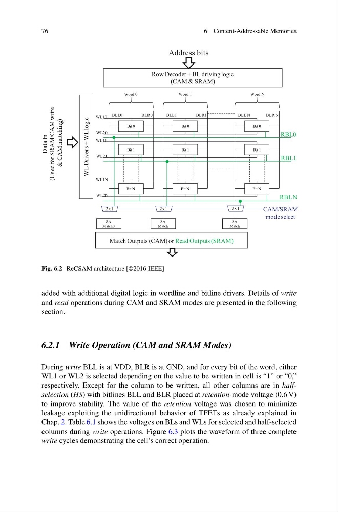
Fig. 6.2 ReCSAM architecture [©2016 IEEE]
added with additional digital logic in wordline and bitline drivers. Details of write
and read operations during CAM and SRAM modes are presented in the following
section.
6.2.1 Write Operation (CAM and SRAM Modes)
During write BLL is at VDD, BLR is at GND, and for every bit of the word, either
WL1 or WL2 is selected depending on the value to be written in cell is “1” or “0,”
respectively. Except for the column to be written, all other columns are in halfselection (HS) with bitlines BLL and BLR placed at retention-mode voltage (0.6 V)
to improve stability. The value of the retention voltage was chosen to minimize
leakage exploiting the unidirectional behavior of TFETs as already explained in
Chap. 2. Table 6.1 shows the voltages on BLs and WLs for selected and half-selected
columns during write operations. Figure 6.3 plots the waveform of three complete
write cycles demonstrating the cell’s correct operation.
6 Content-Addressable Memories
Address bits
Bit 0
Bit 1
Bit N
BLL1
BLR1
Bit 0
Bit 1
Bit N
BLL0
BLR0
Bit 0
Bit 1
Bit N
BLL N
BLR N
SA
Match0
SA
Match
SA
Match
Word 0
Word 1
Word N
WL10
WL20
WL11
WL21
WL1N
WL2N
RBL N
RBL0
RBL1
Row Decoder + BL driving logic
(CAM & SRAM)
WL Drivers + WL logic
Data In
(Used for SRAM/CAM write
& CAM matching)
Match Outputs (CAM) or Read Outputs (SRAM)
2x1
2x1
2x1
CAM/SRAM
mode select
Fig. 6.2 ReCSAM architecture [©2016 IEEE]
added with additional digital logic in wordline and bitline drivers. Details of write
and read operations during CAM and SRAM modes are presented in the following
section.
6.2.1 Write Operation (CAM and SRAM Modes)
During write BLL is at VDD, BLR is at GND, and for every bit of the word, either
WL1 or WL2 is selected depending on the value to be written in cell is “1” or “0,”
respectively. Except for the column to be written, all other columns are in halfselection (HS) with bitlines BLL and BLR placed at retention-mode voltage (0.6 V)
to improve stability. The value of the retention voltage was chosen to minimize
leakage exploiting the unidirectional behavior of TFETs as already explained in
Chap. 2. Table 6.1 shows the voltages on BLs and WLs for selected and half-selected
columns during write operations. Figure 6.3 plots the waveform of three complete
write cycles demonstrating the cell’s correct operation.