

5.4 Comparison and Results
69
0,50
5,00
50,00
500,00
MS
TGFF
C2MOSFF
SAFF
MSAFF
DFF
MOSFET VDD=0.8
MOSFET VDD=0.5
FinFET VDD=0.8
FinFET VDD=0.5
HTFET_FF VDD=0.5
HTFET_FF VDD=0.3
TFET_FF VDD=0.5
TFET_FF VDD=0.3
CMOS_FF VDD=0.5
FinFET_FF VDD=0.5
FinFET_HP_FF VDD=0.3
T
Setup [ps]
simulated
MSFF
values estimated from graphs in literature
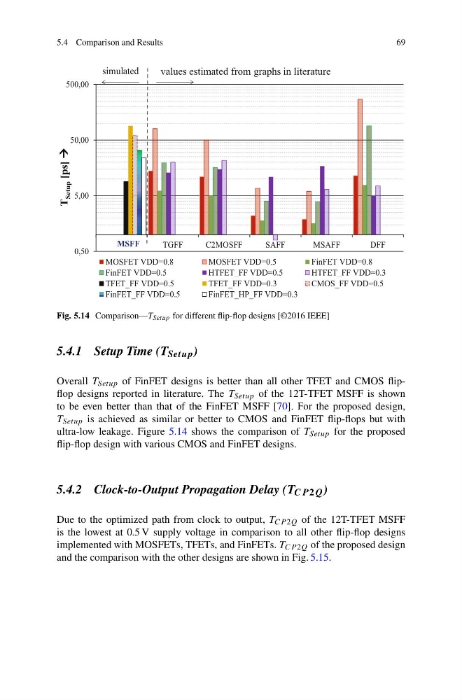
Fig. 5.14 Comparison—T Setup for different flip-flop designs [©2016 IEEE]
5.4.1 Setup Time (T Setup )
Overall T Setup of FinFET designs is better than all other TFET and CMOS flipflop designs reported in literature. The T Setup of the 12T-TFET MSFF is shown
to be even better than that of the FinFET MSFF [70]. For the proposed design,
T Setup is achieved as similar or better to CMOS and FinFET flip-flops but with
ultra-low leakage. Figure 5.14 shows the comparison of T Setup for the proposed
flip-flop design with various CMOS and FinFET designs.
5.4.2 Clock-to-Output Propagation Delay (T CP 2Q )
Due to the optimized path from clock to output, T CP 2Q of the 12T-TFET MSFF
is the lowest at 0.5 V supply voltage in comparison to all other flip-flop designs
implemented with MOSFETs, TFETs, and FinFETs. T CP 2Q of the proposed design
and the comparison with the other designs are shown in Fig. 5.15.
69
0,50
5,00
50,00
500,00
MS
TGFF
C2MOSFF
SAFF
MSAFF
DFF
MOSFET VDD=0.8
MOSFET VDD=0.5
FinFET VDD=0.8
FinFET VDD=0.5
HTFET_FF VDD=0.5
HTFET_FF VDD=0.3
TFET_FF VDD=0.5
TFET_FF VDD=0.3
CMOS_FF VDD=0.5
FinFET_FF VDD=0.5
FinFET_HP_FF VDD=0.3
T
Setup [ps]
simulated
MSFF
values estimated from graphs in literature
Fig. 5.14 Comparison—T Setup for different flip-flop designs [©2016 IEEE]
5.4.1 Setup Time (T Setup )
Overall T Setup of FinFET designs is better than all other TFET and CMOS flipflop designs reported in literature. The T Setup of the 12T-TFET MSFF is shown
to be even better than that of the FinFET MSFF [70]. For the proposed design,
T Setup is achieved as similar or better to CMOS and FinFET flip-flops but with
ultra-low leakage. Figure 5.14 shows the comparison of T Setup for the proposed
flip-flop design with various CMOS and FinFET designs.
5.4.2 Clock-to-Output Propagation Delay (T CP 2Q )
Due to the optimized path from clock to output, T CP 2Q of the 12T-TFET MSFF
is the lowest at 0.5 V supply voltage in comparison to all other flip-flop designs
implemented with MOSFETs, TFETs, and FinFETs. T CP 2Q of the proposed design
and the comparison with the other designs are shown in Fig. 5.15.