

5.3 12T-TFET Master-Slave Flip-Flop (MSFF) Design
65
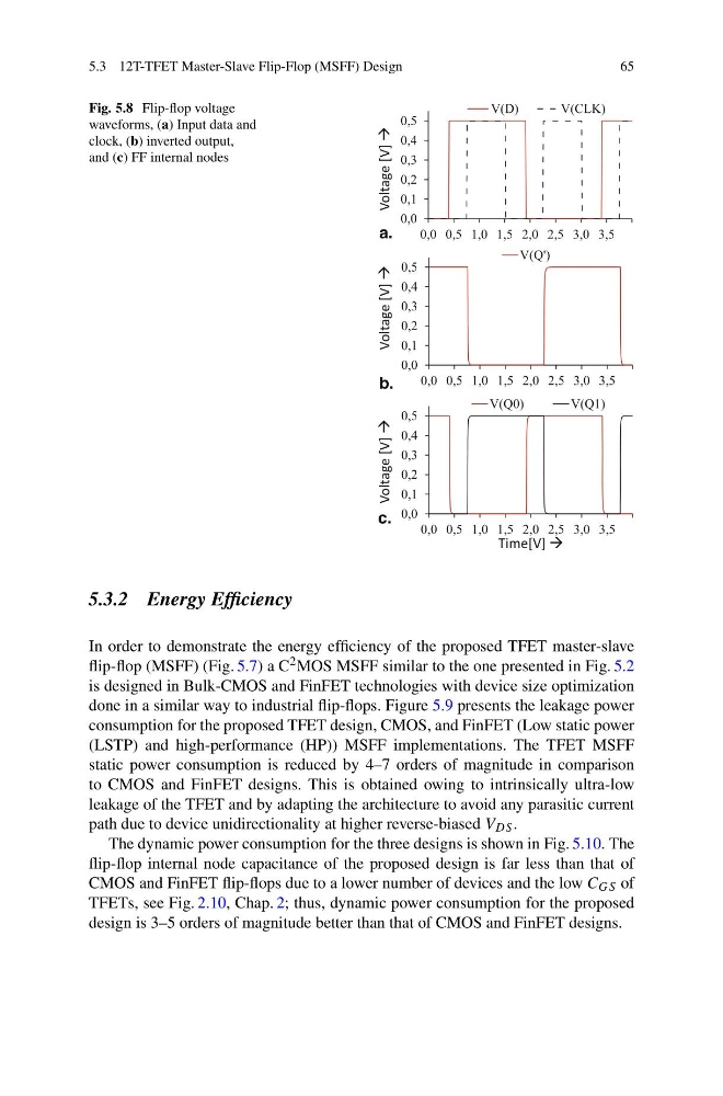
Fig. 5.8 Flip-flop voltage
waveforms, (a) Input data and
clock, (b) inverted output,
and (c) FF internal nodes
0,0
0,1
0,2
0,3
0,4
0,5
0,0 0,5 1,0 1,5 2,0 2,5 3,0 3,5
V(D)
V(CLK)
0,0
0,1
0,2
0,3
0,4
0,5
0,0 0,5 1,0 1,5 2,0 2,5 3,0 3,5
V(Q')
0,0
0,1
0,2
0,3
0,4
0,5
0,0 0,5 1,0 1,5 2,0 2,5 3,0 3,5
V(Q0)
V(Q1)
Voltage [V]
Voltage [V]
Voltage [V]
Time[V]
a.
b.
c.
5.3.2 Energy Efficiency
In order to demonstrate the energy efficiency of the proposed TFET master-slave
flip-flop (MSFF) (Fig. 5.7) a C 2 MOS MSFF similar to the one presented in Fig. 5.2
is designed in Bulk-CMOS and FinFET technologies with device size optimization
done in a similar way to industrial flip-flops. Figure 5.9 presents the leakage power
consumption for the proposed TFET design, CMOS, and FinFET (Low static power
(LSTP) and high-performance (HP)) MSFF implementations. The TFET MSFF
static power consumption is reduced by 4–7 orders of magnitude in comparison
to CMOS and FinFET designs. This is obtained owing to intrinsically ultra-low
leakage of the TFET and by adapting the architecture to avoid any parasitic current
path due to device unidirectionality at higher reverse-biased V DS .
The dynamic power consumption for the three designs is shown in Fig. 5.10. The
flip-flop internal node capacitance of the proposed design is far less than that of
CMOS and FinFET flip-flops due to a lower number of devices and the low C GS of
TFETs, see Fig. 2.10, Chap. 2; thus, dynamic power consumption for the proposed
design is 3–5 orders of magnitude better than that of CMOS and FinFET designs.
65
Fig. 5.8 Flip-flop voltage
waveforms, (a) Input data and
clock, (b) inverted output,
and (c) FF internal nodes
0,0
0,1
0,2
0,3
0,4
0,5
0,0 0,5 1,0 1,5 2,0 2,5 3,0 3,5
V(D)
V(CLK)
0,0
0,1
0,2
0,3
0,4
0,5
0,0 0,5 1,0 1,5 2,0 2,5 3,0 3,5
V(Q')
0,0
0,1
0,2
0,3
0,4
0,5
0,0 0,5 1,0 1,5 2,0 2,5 3,0 3,5
V(Q0)
V(Q1)
Voltage [V]
Voltage [V]
Voltage [V]
Time[V]
a.
b.
c.
5.3.2 Energy Efficiency
In order to demonstrate the energy efficiency of the proposed TFET master-slave
flip-flop (MSFF) (Fig. 5.7) a C 2 MOS MSFF similar to the one presented in Fig. 5.2
is designed in Bulk-CMOS and FinFET technologies with device size optimization
done in a similar way to industrial flip-flops. Figure 5.9 presents the leakage power
consumption for the proposed TFET design, CMOS, and FinFET (Low static power
(LSTP) and high-performance (HP)) MSFF implementations. The TFET MSFF
static power consumption is reduced by 4–7 orders of magnitude in comparison
to CMOS and FinFET designs. This is obtained owing to intrinsically ultra-low
leakage of the TFET and by adapting the architecture to avoid any parasitic current
path due to device unidirectionality at higher reverse-biased V DS .
The dynamic power consumption for the three designs is shown in Fig. 5.10. The
flip-flop internal node capacitance of the proposed design is far less than that of
CMOS and FinFET flip-flops due to a lower number of devices and the low C GS of
TFETs, see Fig. 2.10, Chap. 2; thus, dynamic power consumption for the proposed
design is 3–5 orders of magnitude better than that of CMOS and FinFET designs.