

62
5 TFET NDR Flip-Flop
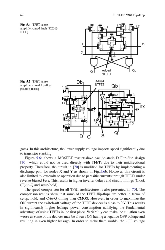
Fig. 5.4 TFET sense
amplifier-based latch [©2013
IEEE]
D
C
Q
Qb
Db
1.7
1.7
1.7
1.7
3
3
3
3
1
3
Added
NTFET
Fig. 5.5 TFET sense
amplifier-based flip-flop
[©2013 IEEE]
gates. In this architecture, the lower supply voltage impacts speed significantly due
to transistor stacking.
Figure 5.6a shows a MOSFET master-slave pseudo-static D Flip-flop design
[70], which could not be used directly with TFETs due to their unidirectional
property. Therefore, the circuit in [70] is modified for TFETs by implementing a
discharge path for nodes X and Y as shown in Fig. 5.6b. However, this circuit is
also limited to low-voltage operation due to parasitic currents through TFETs under
reverse-biased V DS . This results in higher inverter delays and circuit timings (Clock
(C)-to-Q and setup/hold).
The speed comparison for all TFET architectures is also presented in [70]. The
comparison results show that some of the TFET flip-flops are better in terms of
setup, hold, and C-to-Q timing than CMOS. However, in order to maximize the
ON current the switch-off voltage of the TFET devices is close to 0 V. This results
in significantly higher leakage power consumption nullifying the fundamental
advantage of using TFETs in the first place. Variability can make the situation even
worse as some of the devices may be always ON having a negative OFF voltage and
resulting in even higher leakage. In order to make them usable, the OFF voltage
5 TFET NDR Flip-Flop
Fig. 5.4 TFET sense
amplifier-based latch [©2013
IEEE]
D
C
Q
Qb
Db
1.7
1.7
1.7
1.7
3
3
3
3
1
3
Added
NTFET
Fig. 5.5 TFET sense
amplifier-based flip-flop
[©2013 IEEE]
gates. In this architecture, the lower supply voltage impacts speed significantly due
to transistor stacking.
Figure 5.6a shows a MOSFET master-slave pseudo-static D Flip-flop design
[70], which could not be used directly with TFETs due to their unidirectional
property. Therefore, the circuit in [70] is modified for TFETs by implementing a
discharge path for nodes X and Y as shown in Fig. 5.6b. However, this circuit is
also limited to low-voltage operation due to parasitic currents through TFETs under
reverse-biased V DS . This results in higher inverter delays and circuit timings (Clock
(C)-to-Q and setup/hold).
The speed comparison for all TFET architectures is also presented in [70]. The
comparison results show that some of the TFET flip-flops are better in terms of
setup, hold, and C-to-Q timing than CMOS. However, in order to maximize the
ON current the switch-off voltage of the TFET devices is close to 0 V. This results
in significantly higher leakage power consumption nullifying the fundamental
advantage of using TFETs in the first place. Variability can make the situation even
worse as some of the devices may be always ON having a negative OFF voltage and
resulting in even higher leakage. In order to make them usable, the OFF voltage