

5.2 State-of-the-Art TFET Flip-Flops
61
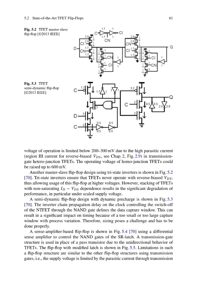
Fig. 5.2 TFET master-slave
flip-flop [©2013 IEEE]
Fig. 5.3 TFET
semi-dynamic flip-flop
[©2013 IEEE]
voltage of operation is limited below 200–300 mV due to the high parasitic current
(region III current for reverse-biased V DS , see Chap. 2, Fig. 2.9) in transmissiongate hetero-junction TFETs. The operating voltage of homo-junction TFETs could
be raised up to 600 mV.
Another master-slave flip-flop design using tri-state inverters is shown in Fig. 5.2
[70]. Tri-state inverters ensure that TFETs never operate with reverse-biased V DS ,
thus allowing usage of this flip-flop at higher voltages. However, stacking of TFETs
with non-saturating I D − V DS dependence results in the significant degradation of
performance, in particular under scaled supply voltage.
A semi-dynamic flip-flop design with dynamic precharge is shown in Fig. 5.3
[70]. The inverter chain propagation delay on the clock controlling the switch-off
of the NTFET through the NAND gate defines the data capture window. This can
result in a significant impact on timing because of a too small or too large capture
window with process variation. Therefore, sizing poses a challenge and has to be
done properly.
A sense-amplifier-based flip-flop is shown in Fig. 5.4 [70] using a differential
sense amplifier to control the NAND gates of the SR-latch. A transmission-gate
structure is used in place of a pass transistor due to the unidirectional behavior of
TFETs. The flip-flop with modified latch is shown in Fig. 5.5. Limitations in such
a flip-flop structure are similar to the other flip-flop structures using transmission
gates, i.e., the supply voltage is limited by the parasitic current through transmission
61
Fig. 5.2 TFET master-slave
flip-flop [©2013 IEEE]
Fig. 5.3 TFET
semi-dynamic flip-flop
[©2013 IEEE]
voltage of operation is limited below 200–300 mV due to the high parasitic current
(region III current for reverse-biased V DS , see Chap. 2, Fig. 2.9) in transmissiongate hetero-junction TFETs. The operating voltage of homo-junction TFETs could
be raised up to 600 mV.
Another master-slave flip-flop design using tri-state inverters is shown in Fig. 5.2
[70]. Tri-state inverters ensure that TFETs never operate with reverse-biased V DS ,
thus allowing usage of this flip-flop at higher voltages. However, stacking of TFETs
with non-saturating I D − V DS dependence results in the significant degradation of
performance, in particular under scaled supply voltage.
A semi-dynamic flip-flop design with dynamic precharge is shown in Fig. 5.3
[70]. The inverter chain propagation delay on the clock controlling the switch-off
of the NTFET through the NAND gate defines the data capture window. This can
result in a significant impact on timing because of a too small or too large capture
window with process variation. Therefore, sizing poses a challenge and has to be
done properly.
A sense-amplifier-based flip-flop is shown in Fig. 5.4 [70] using a differential
sense amplifier to control the NAND gates of the SR-latch. A transmission-gate
structure is used in place of a pass transistor due to the unidirectional behavior of
TFETs. The flip-flop with modified latch is shown in Fig. 5.5. Limitations in such
a flip-flop structure are similar to the other flip-flop structures using transmission
gates, i.e., the supply voltage is limited by the parasitic current through transmission