

60
5 TFET NDR Flip-Flop
An ultra-compact flip-flop design using Si-TFETs for ULP application focusing
on area and power efficiency using the Negative Differential Resistance (NDR) and
unidirectionality properties of TFETs, see Chap. 2 [14], is presented in Sect. 5.3.
The design-level issues in TFET flip-flops are analyzed and a novel 12T-TFET
master-slave flip-flop (MSFF) cell designed using the NDR property of TFETs in
reverse bias [14] is demonstrated. The used TFETs are compatible with CMOS
for fabrication allowing the implementation of heterogeneous cores within a single
FDSOI-CMOS process using both TFET and CMOS devices.
5.2 State-of-the-Art TFET Flip-Flops
Due to TFET’s characteristics being different than those of CMOS, flip-flop architectures require additional modifications than the simple replacement of MOSFETs
with TFETs. Transmission gate, master-slave, semi-dynamic, sense amplifier, and
pseudo-static flip-flop architectures are presented in [70].
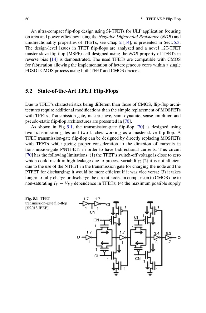
As shown in Fig. 5.1, the transmission-gate flip-flop [70] is designed using
two transmission gates and two latches working as a master-slave flip-flop. A
TFET transmission-gate flip-flop can be designed by directly replacing MOSFETs
with TFETs while giving proper consideration to the direction of currents in
transmission-gate P/NTFETs in order to have bidirectional currents. This circuit
[70] has the following limitations: (1) the TFET’s switch-off voltage is close to zero
which could result in high leakage due to process variability; (2) it is not efficient
due to the use of the NTFET in the transmission gate for charging the node and the
PTFET for discharging; it would be more efficient if it was vice versa; (3) it takes
longer to fully charge or discharge the circuit nodes in comparison to CMOS due to
non-saturating I D − V DS dependence in TFETs; (4) the maximum possible supply
Fig. 5.1 TFET
transmission-gate flip-flop
[©2013 IEEE]
1.7
1.7
1.7
1.7
CN
Q
6.3
3.4
1.7
D
CN
CN
CI
CI
CI
1
1
1
1
1
1
1
1
1
1
1
1
1
2
1
1
1
5 TFET NDR Flip-Flop
An ultra-compact flip-flop design using Si-TFETs for ULP application focusing
on area and power efficiency using the Negative Differential Resistance (NDR) and
unidirectionality properties of TFETs, see Chap. 2 [14], is presented in Sect. 5.3.
The design-level issues in TFET flip-flops are analyzed and a novel 12T-TFET
master-slave flip-flop (MSFF) cell designed using the NDR property of TFETs in
reverse bias [14] is demonstrated. The used TFETs are compatible with CMOS
for fabrication allowing the implementation of heterogeneous cores within a single
FDSOI-CMOS process using both TFET and CMOS devices.
5.2 State-of-the-Art TFET Flip-Flops
Due to TFET’s characteristics being different than those of CMOS, flip-flop architectures require additional modifications than the simple replacement of MOSFETs
with TFETs. Transmission gate, master-slave, semi-dynamic, sense amplifier, and
pseudo-static flip-flop architectures are presented in [70].
As shown in Fig. 5.1, the transmission-gate flip-flop [70] is designed using
two transmission gates and two latches working as a master-slave flip-flop. A
TFET transmission-gate flip-flop can be designed by directly replacing MOSFETs
with TFETs while giving proper consideration to the direction of currents in
transmission-gate P/NTFETs in order to have bidirectional currents. This circuit
[70] has the following limitations: (1) the TFET’s switch-off voltage is close to zero
which could result in high leakage due to process variability; (2) it is not efficient
due to the use of the NTFET in the transmission gate for charging the node and the
PTFET for discharging; it would be more efficient if it was vice versa; (3) it takes
longer to fully charge or discharge the circuit nodes in comparison to CMOS due to
non-saturating I D − V DS dependence in TFETs; (4) the maximum possible supply
Fig. 5.1 TFET
transmission-gate flip-flop
[©2013 IEEE]
1.7
1.7
1.7
1.7
CN
Q
6.3
3.4
1.7
D
CN
CN
CI
CI
CI
1
1
1
1
1
1
1
1
1
1
1
1
1
2
1
1
1