

4.5 Summary
55
DL
DLB
ML-search miss
ML-search hit
Start of CAM search
Voltage [mV]
Voltage [mV]
Time [ns]
650.0
550.0
450.0
350.0
250.0
150.0
50.0
650.0
500.0
400.0
300.0
200.0
0.6
1.0
1.4
1.8
2.2
2.6
–50.0
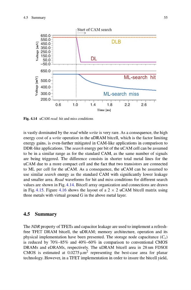
Fig. 4.14 uCAM read: hit and miss conditions
is vastly dominated by the read while write is very rare. As a consequence, the high
energy cost of a write operation in the uDRAM bitcell, which is the factor limiting
energy gains, is even-further mitigated in CAM-like applications in comparison to
DDR-like applications. The search energy per bit of the uCAM cell can be assumed
to be in a similar range as for the standard CAM, as the same number of signals
are being triggered. The difference consists in shorter total metal lines for the
uCAM due to a more compact cell and the fact that two transistors are connected
to ML per cell for the uCAM. As a consequence, the uCAM can be assumed to
use similar search energy as the standard CAM with significantly lower leakage
and smaller area. Read waveforms for hit and miss conditions for different search
values are shown in Fig. 4.14. Bitcell array organization and connections are drawn
in Fig. 4.15. Figure 4.16 shows the layout of a 2 × 2 uCAM bitcell matrix using
three metals with virtual ground G in the above metal layer.
4.5 Summary
The NDR property of TFETs and capacitor leakage are used to implement a refreshfree TFET DRAM bitcell, the uDRAM; memory architecture, operation and its
physical implementation have been presented. The storage node capacitance (C s )
is reduced by 70%–85% and 40%–60% in comparison to conventional CMOS
DRAMs and eDRAMs, respectively. The uDRAM bitcell area in 28 nm FDSOI
CMOS is estimated at 0.0275 µm 2 representing the best-case area for planar
technology. However, in a TFET implementation in order to insure the bitcell yield,
55
DL
DLB
ML-search miss
ML-search hit
Start of CAM search
Voltage [mV]
Voltage [mV]
Time [ns]
650.0
550.0
450.0
350.0
250.0
150.0
50.0
650.0
500.0
400.0
300.0
200.0
0.6
1.0
1.4
1.8
2.2
2.6
–50.0
Fig. 4.14 uCAM read: hit and miss conditions
is vastly dominated by the read while write is very rare. As a consequence, the high
energy cost of a write operation in the uDRAM bitcell, which is the factor limiting
energy gains, is even-further mitigated in CAM-like applications in comparison to
DDR-like applications. The search energy per bit of the uCAM cell can be assumed
to be in a similar range as for the standard CAM, as the same number of signals
are being triggered. The difference consists in shorter total metal lines for the
uCAM due to a more compact cell and the fact that two transistors are connected
to ML per cell for the uCAM. As a consequence, the uCAM can be assumed to
use similar search energy as the standard CAM with significantly lower leakage
and smaller area. Read waveforms for hit and miss conditions for different search
values are shown in Fig. 4.14. Bitcell array organization and connections are drawn
in Fig. 4.15. Figure 4.16 shows the layout of a 2 × 2 uCAM bitcell matrix using
three metals with virtual ground G in the above metal layer.
4.5 Summary
The NDR property of TFETs and capacitor leakage are used to implement a refreshfree TFET DRAM bitcell, the uDRAM; memory architecture, operation and its
physical implementation have been presented. The storage node capacitance (C s )
is reduced by 70%–85% and 40%–60% in comparison to conventional CMOS
DRAMs and eDRAMs, respectively. The uDRAM bitcell area in 28 nm FDSOI
CMOS is estimated at 0.0275 µm 2 representing the best-case area for planar
technology. However, in a TFET implementation in order to insure the bitcell yield,